- 您现在的位置:买卖IC网 > PDF目录271233 > S29CL016J0JFFI130 (SPANSION LLC) 512K X 32 FLASH 3.3V PROM, 54 ns, PBGA80 PDF资料下载
参数资料
| 型号: | S29CL016J0JFFI130 |
| 厂商: | SPANSION LLC |
| 元件分类: | PROM |
| 英文描述: | 512K X 32 FLASH 3.3V PROM, 54 ns, PBGA80 |
| 封装: | 13 X 11 MM, 1 MM PITCH, LEAD FREE, FORTIFIED, BGA-80 |
| 文件页数: | 72/78页 |
| 文件大小: | 1825K |
| 代理商: | S29CL016J0JFFI130 |
第1页第2页第3页第4页第5页第6页第7页第8页第9页第10页第11页第12页第13页第14页第15页第16页第17页第18页第19页第20页第21页第22页第23页第24页第25页第26页第27页第28页第29页第30页第31页第32页第33页第34页第35页第36页第37页第38页第39页第40页第41页第42页第43页第44页第45页第46页第47页第48页第49页第50页第51页第52页第53页第54页第55页第56页第57页第58页第59页第60页第61页第62页第63页第64页第65页第66页第67页第68页第69页第70页第71页当前第72页第73页第74页第75页第76页第77页第78页
72
S29CD-J & S29CL-J Flash Family
S29CD-J_CL-J_00_B1 September27,2006
Prel imi n ary
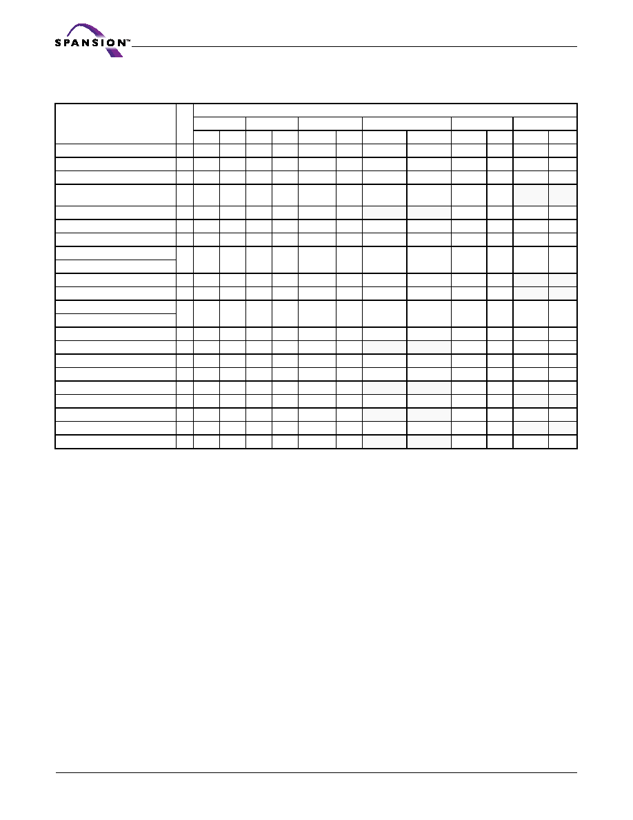
Table 20.2 Sector Protection Command Definitions (x32 Mode)
Command (Notes)
Cy
cl
es
First
Second
Third
Fourth
Fifth
Sixth
Addr
Data
Addr
Data
Addr
Data
Addr
Data
Addr
Data
Addr
Data
Reset
1
XXX
F0
Secured Silicon Sector Entry
3
555
AA
2AA
55
555
88
Secured Silicon Sector Exit
4
555
AA
2AA
55
555
90
XX
00
Secured Silicon Protection
Bit Program (5, 6)
6
555
AA
2AA
55
555
60
OW
68
OW
48
OW
RD(0)
Secured Silicon Protection Bit Status
6
555
AA
2AA
55
555
60
OW
RD(0)
Password Program (5, 7, 8)
4
555
AA
2AA
55
555
38
PWA[0-1]
PWD[0-1]
Password Verify
4
555
AA
2AA
55
555
C8
PWA[0-1]
PWD[0-1]
Password Unlock (7, 8)
5
555
AA
2AA
55
555
28
PWA[0-1]
PWD[0-1]
6
555
AA
2AA
55
555
60
SG+WP
68
SG+WP
48
SG+WP
RD(0)
All PPB Erase (5, 9, 10)
6
555
AA
2AA
55
555
60
WP
60
WP
40
WP
RD(0)
PPB Status (11, 12)
4
555
AA
2AA
55
BA+555
90
SA+X02
00/01
PPB Lock Bit Set
3
555
AA
2AA
55
555
78
PPB Lock Bit Status
4
555
AA
2AA
55
BA+555
58
SA
RD(1)
DYB Write (7)
4
555
AA
2AA
55
555
48
SA
X1
DYB Erase (7)
4
555
AA
2AA
55
555
48
SA
X0
DYB Status (12)
4
555
AA
2AA
55
BA+555
58
SA
RD(0)
PPMLB Program (5, 6)
6
555
AA
2AA
55
555
60
PL
68
PL
48
PL
RD(0)
PPMLB Status (5)
6
555
AA
2AA
55
555
60
PL
RD(0)
SPMLB Program (5, 6)
6
555
AA
2AA
55
555
60
SL
68
SL
48
SL
RD(0)
SPMLB Status (5)
6
555
AA
2AA
55
555
60
SL
RD(0)
Legend:
DYB = Dynamic Protection Bit
OW = Address (A5–A0) is (011X10).
PPB = Persistent Protection Bit
PWA = Password Address. A0 selects between the low and high 32-bit
portions of the 64-bit Password
PWD = Password Data. Must be written over two cycles.
PL = Password Protection Mode Lock Address (A5–A0) is (001X10)
RD(0) = Read Data DQ0 protection indicator bit. If protected, DQ0= 1,
if unprotected, DQ0 = 0.
RD(1) = Read Data DQ1 protection indicator bit. If protected, DQ1 =
1, if unprotected, DQ1 = 0.
SA = Sector Address. The set of addresses that comprise a sector. The
system may write any address within a sector to identify that sector
for a command.
SG = Sector Group Address
BA = Bank Address. The set of addresses that comprise a bank. The
system may write any address within a bank to identify that bank for a
command.
SL = Persistent Protection Mode Lock Address (A5–A0) is (010X10)
WP = PPB Address (A5–A0) is (111010)
X = Don’t care
PPMLB = Password Protection Mode Locking Bit
SPMLB = Persistent Protection Mode Locking Bit
Notes:
1. See Table 8.1 for description of bus operations.
2. All values are in hexadecimal.
3. Shaded cells in table denote read cycles. All other cycles are
write operations.
4. During unlock cycles, (lower address bits are 555 or 2AAh as
shown in table) address bits higher than A11 (except where BA
is required) and data bits higher than DQ7 are don’t cares.
5. The reset command returns the device to reading the array.
6. The fourth cycle programs the addressed locking bit. The fifth
and sixth cycles are used to validate whether the bit has been
fully programmed. If DQ0 (in the sixth cycle) reads 0, the
program command must be issued and verified again.
7. Data is latched on the rising edge of WE#.
8. The entire four bus-cycle sequence must be entered for each
portion of the password.
9. The fourth cycle erases all PPBs. The fifth and sixth cycles are
used to validate whether the bits have been fully erased. If DQ0
(in the sixth cycle) reads 1, the erase command must be issued
and verified again.
10. Before issuing the erase command, all PPBs should be
programmed in order to prevent over-erasure of PPBs.
11. In the fourth cycle, 00h indicates PPB set; 01h indicates PPB not
set.
12. The status of additional PPBs and DYBs may be read (following
the fourth cycle) without reissuing the entire command
sequence.
相关PDF资料 |
PDF描述 |
|---|---|
| S29CL016J0MQAI113 | 512K X 32 FLASH 3.3V PROM, 54 ns, PQFP80 |
| S29CL016J0PQFI123 | 512K X 32 FLASH 3.3V PROM, 54 ns, PQFP80 |
| S29CL016J1MFAI123 | 512K X 32 FLASH 3.3V PROM, 54 ns, PBGA80 |
| S29CL016J1MFFI030 | 512K X 32 FLASH 3.3V PROM, 54 ns, PBGA80 |
| S29CL016J0JQFI022 | 512K X 32 FLASH 3.3V PROM, 54 ns, PQFP80 |
相关代理商/技术参数 |
参数描述 |
|---|---|
| S29CL016J0JQFM030 | 制造商:Spansion 功能描述:FLASH PARALLEL 3.3V 16MBIT 512KX32 54NS 80PQFP - Trays |
| S29CL016J0JQFM030P | 制造商:Spansion 功能描述:AUTO 3.3V 512KX32 FLASH - Trays |
| S29CL016J0JQFM030U | 制造商:Spansion 功能描述:32M (4MX8/2MX16) 3V REG, MIRRORBIT, TOP, FBGA48, IND - Trays |
| S29CL016J0JQFM03U | 制造商:Spansion 功能描述:32M (4MX8/2MX16) 3V REG, MIRRORBIT, TOP, FBGA48, IND - Trays |
| S29CL016J0MQFM030 | 制造商:Spansion 功能描述: |
发布紧急采购,3分钟左右您将得到回复。