- 您现在的位置:买卖IC网 > PDF目录270895 > S29GL032M10TFIR10 (SPANSION LLC) MirrorBit Flash Family PDF资料下载
参数资料
| 型号: | S29GL032M10TFIR10 |
| 厂商: | SPANSION LLC |
| 元件分类: | PROM |
| 英文描述: | MirrorBit Flash Family |
| 中文描述: | 2M X 16 FLASH 3V PROM, 100 ns, PDSO56 |
| 封装: | LEAD FREE, MO-142EC, TSOP-56 |
| 文件页数: | 3/116页 |
| 文件大小: | 6024K |
| 代理商: | S29GL032M10TFIR10 |
第1页第2页当前第3页第4页第5页第6页第7页第8页第9页第10页第11页第12页第13页第14页第15页第16页第17页第18页第19页第20页第21页第22页第23页第24页第25页第26页第27页第28页第29页第30页第31页第32页第33页第34页第35页第36页第37页第38页第39页第40页第41页第42页第43页第44页第45页第46页第47页第48页第49页第50页第51页第52页第53页第54页第55页第56页第57页第58页第59页第60页第61页第62页第63页第64页第65页第66页第67页第68页第69页第70页第71页第72页第73页第74页第75页第76页第77页第78页第79页第80页第81页第82页第83页第84页第85页第86页第87页第88页第89页第90页第91页第92页第93页第94页第95页第96页第97页第98页第99页第100页第101页第102页第103页第104页第105页第106页第107页第108页第109页第110页第111页第112页第113页第114页第115页第116页
98
S29GL-M MirrorBitTM Flash Family
S29GL-M_00_B8 February 7, 2007
Data
Sheet
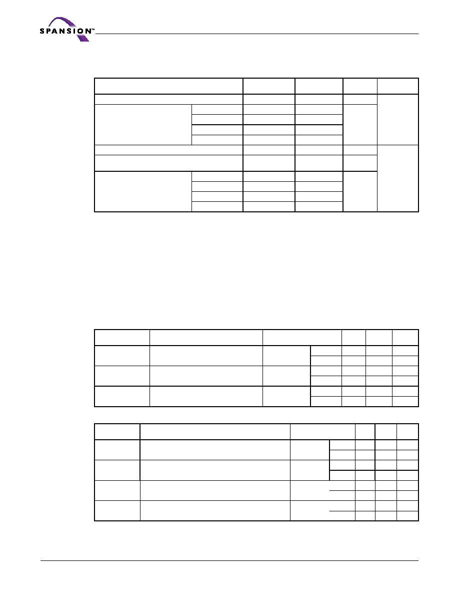
Erase and Programming Performance
Notes:
1. Typical program and erase times assume the following conditions: 25°C, VCC = 3.0V, 10,000
cycles; checkerboard data pattern.
2. Under worst case conditions of 90
°C; Worst case VCC, 100,000 cycles.
3. Effective programming time (typ) is 15 μs (per word), 7.5 μs (per byte).
4. Effective accelerated programming time (typ) is 12.5 μs (per word), 6.3 μs (per byte).
5. Effective write buffer specification is calculated on a per-word/per-byte basis for a 16-word/32-
byte write buffer operation.
6. In the pre-programming step of the Embedded Erase algorithm, all bits are programmed to 00h
before erasure.
7. System-level overhead is the time required to execute the command sequence(s) for the program
TSOP Pin and BGA Package Capacitance
For package types TA, TF, BA, BF, FA, FF (refer to Ordering Information Pages):
For package types TB, TC, BB, BC, (refer to Ordering Information Pages):
Notes:
1. Sampled, not 100% tested.
2. Test conditions TA = 25°C, f = 1.0 MHz.
Parameter
(Notes)
Typ
Max
Unit
Comments
Sector Erase Time
0.5
3.5
sec
Excludes 00h
programming
prior to
erasure
Chip Erase Time
S29GL032M
32
64
sec
S29GL064M
64
128
S29GL128M
128
256
S29GL256M
256
512
Total Write Buffer Program Time (3, 5)
240
s
Excludes
system level
overhead
Total Accelerated Effective Write Buffer Program Time
200
s
Chip Program Time
S29GL032M
31.5
sec
S29GL064M
63
S29GL128M
126
S29GL256M
252
Parameter
Symbol
Parameter
Description
Test
Setup
Typ
Max
Unit
CIN
Input Capacitance
VIN = 0
TSOP
6
7.5
pF
BGA
4.2
5.0
pF
COUT
Output Capacitance
VOUT = 0
TSOP
8.5
12
pF
BGA
5.4
6.5
pF
CIN2
Control Pin Capacitance
VIN = 0
TSOP
7.5
9
pF
BGA
3.9
4.7
pF
Parameter
Symbol
Parameter
Description
Test
Setup
Typ
Max
Unit
CIN
Input Capacitance
VIN = 0
TSOP
8
10
pF
BGA
8
10
pF
COUT
Output Capacitance
VOUT = 0
TSOP
8.5
12
pF
BGA
8.5
12
pF
CIN2
Control Pin Capacitance
VIN = 0
TSOP
8
10
pF
BGA
8
10
pF
CIN3
RESET# and WP#/ACC Pin Capacitance
VIN = 0
TSOP
20
25
pF
BGA
15
20
pF
相关PDF资料 |
PDF描述 |
|---|---|
| S29GL032M10BFIR10 | MirrorBit Flash Family |
| S29GL032A10TFIR10 | 64 MEGABIT 32MEGABIT 3.0 BOLT ONLY PAGE MODE FLASH MEMORY |
| S29GL032A11BFIR10 | 64 MEGABIT 32MEGABIT 3.0 BOLT ONLY PAGE MODE FLASH MEMORY |
| S29AL016M90BFIR10 | 16 MEGABIT (2M X 8 BIT / I M X 16 BIT) 3.0 VOLT ONLY BOOT SECTOR FLASH MEMORY |
| S29AL016M10BFIR10 | 16 MEGABIT (2M X 8 BIT / I M X 16 BIT) 3.0 VOLT ONLY BOOT SECTOR FLASH MEMORY |
相关代理商/技术参数 |
参数描述 |
|---|---|
| S29GL032M10TFIR12 | 制造商:SPANSION 制造商全称:SPANSION 功能描述:MirrorBit Flash Family |
| S29GL032M10TFIR13 | 制造商:SPANSION 制造商全称:SPANSION 功能描述:MirrorBit Flash Family |
| S29GL032M10TFIR20 | 制造商:SPANSION 制造商全称:SPANSION 功能描述:3.0 Volt-only Page Mode Flash Memory featuring 0.23 um MirrorBit process technology |
| S29GL032M10TFIR22 | 制造商:SPANSION 制造商全称:SPANSION 功能描述:MirrorBit Flash Family |
| S29GL032M10TFIR23 | 制造商:SPANSION 制造商全称:SPANSION 功能描述:MirrorBit Flash Family |
发布紧急采购,3分钟左右您将得到回复。