- 您现在的位置:买卖IC网 > PDF目录96803 > S3096-02 PIN PHOTO DIODE PDF资料下载
参数资料
| 型号: | S3096-02 |
| 元件分类: | 光敏二极管 |
| 英文描述: | PIN PHOTO DIODE |
| 封装: | PLASTIC PACKAGE-4 |
| 文件页数: | 3/3页 |
| 文件大小: | 246K |
| 代理商: | S3096-02 |
www.hamamatsu.com
Information furnished by HAMAMATSU is believed to be reliable. However, no responsibility is assumed for possible inaccuracies or omissions.
Specifications are subject to change without notice. No patent rights are granted to any of the circuits described herein. 2010 Hamamatsu Photonics K.K.
HAMAMATSU PHOTONICS K.K., Solid State Division
1126-1 Ichino-cho, Higashi-ku, Hamamatsu City, 435-8558 Japan, Telephone: (81) 53-434-3311, Fax: (81) 53-434-5184
U.S.A.: Hamamatsu Corporation: 360 Foothill Road, P.O.Box 6910, Bridgewater, N.J. 08807-0910, U.S.A., Telephone: (1) 908-231-0960, Fax: (1) 908-231-1218
Germany: Hamamatsu Photonics Deutschland GmbH: Arzbergerstr. 10, D-82211 Herrsching am Ammersee, Germany, Telephone: (49) 08152-3750, Fax: (49) 08152-2658
France: Hamamatsu Photonics France S.A.R.L.: 19, Rue du Saule Trapu, Parc du Moulin de Massy, 91882 Massy Cedex, France, Telephone: 33-(1) 69 53 71 00, Fax: 33-(1) 69 53 71 10
United Kingdom: Hamamatsu Photonics UK Limited: 2 Howard Court, 10 Tewin Road, Welwyn Garden City, Hertfordshire AL7 1BW, United Kingdom, Telephone: (44) 1707-294888, Fax: (44) 1707-325777
North Europe: Hamamatsu Photonics Norden AB: Smidesvgen 12, SE-171 41 Solna, Sweden, Telephone: (46) 8-509-031-00, Fax: (46) 8-509-031-01
Italy: Hamamatsu Photonics Italia S.R.L.: Strada della Moia, 1/E, 20020 Arese, (Milano), Italy, Telephone: (39) 02-935-81-733, Fax: (39) 02-935-81-741
Cat. No. KMPD1039E04 Nov. 2010 DN
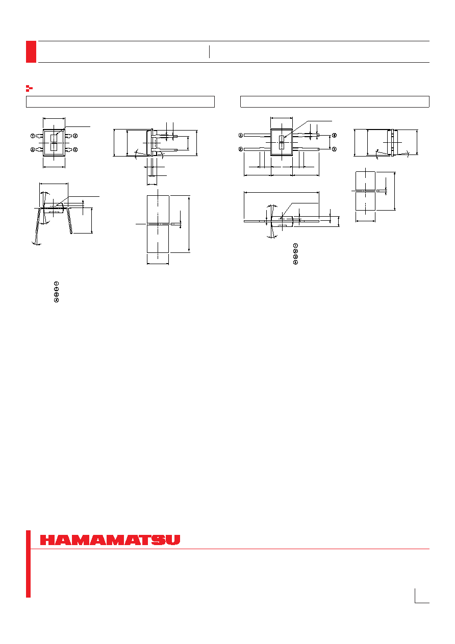
Si PIN photodiodes
S3096-02, S4204
3
KMPDA0119EB
KMPDA0120EB
Dimensional outlines (unit: mm, tolerance unless otherwise noted: ±0.1)
S3096-02
S4204
Chip position accuracy with respect
to the package dimensions marked *
X, Y ≤ ±0.2
θ≤ ±2°
Lead surface finish: Silver plating
Packing: Stick (50 pcs/stick)
Anode A
Cathode common
Anode B
Cathode common
Active area
4.1 ± 0.2
(Including burr)
0.5
2.54
5.2 ± 0.2
4.0 *
0.8
0.25
4.5
±
0.3
Photosensitive
surface
5°
10°
5.0
±
0.2
(Including
burr)
4.8
*
4.7
*
Details of
active area
3.0
1.2
0.03
7.5° ± 5°
1.8
0.6
0.5
A
B
10°
5°
Active area
4.1 ± 0.2
(Including burr)
0.02
2.0
2.54
(0.8)
(1.25)
4.9 ± 0.4
4.0 *
(1.25)
(0.8)
13.8 ± 0.3
4.9 ± 0.4
5°
0.25
10°
0.5
0.8
1.8
5.0
±
0.2
(Including
burr)
4.7
*
4.8
*
5°
10°
Details of
active area
1.0
0.6
0.5
Photosensitive
surface
A
B
Chip position accuracy with respect
tothe package dimensions marked *
X, Y ≤ ±0.2
θ≤ ±2°
Lead surface finish: Silver plating
Packing: Stick (50 pcs/stick)
Anode A
Cathode common
Anode B
Cathode common
相关PDF资料 |
PDF描述 |
|---|---|
| S422-0006-A3 | ACTIVE DELAY LINE, TRUE OUTPUT, PDSO8 |
| S422-0010-10 | ACTIVE DELAY LINE, TRUE OUTPUT, PDSO14 |
| S422-0300-06 | ACTIVE DELAY LINE, TRUE OUTPUT, PDSO4 |
| S422-0500-06 | ACTIVE DELAY LINE, TRUE OUTPUT, PDSO4 |
| S422-0175-06 | ACTIVE DELAY LINE, TRUE OUTPUT, PDSO4 |
相关代理商/技术参数 |
参数描述 |
|---|---|
| S3096-180BK | 制造商:Belden Inc 功能描述:AO Smith Electrical Products company |
| S3098CB12 | 制造商:AMC 功能描述: |
| S3098G2N | 制造商:TYAN 功能描述:PENTIUM M (2) 10/100 LAN; FLEXATX - Bulk |
| S3098G2N RPL | 制造商:TYAN 功能描述:REPAIR/REPLACEMENT - Bulk |
| S3098G2N-DF | 制造商:TYAN 功能描述:TYAN MOTHERBOARD - Bulk |
发布紧急采购,3分钟左右您将得到回复。