- 您现在的位置:买卖IC网 > PDF目录29145 > S4011-04 PHOTO DIODE PDF资料下载
参数资料
| 型号: | S4011-04 |
| 元件分类: | 光敏二极管 |
| 英文描述: | PHOTO DIODE |
| 封装: | PLASTIC PACKAGE-4 |
| 文件页数: | 4/4页 |
| 文件大小: | 773K |
| 代理商: | S4011-04 |
www.hamamatsu.com
Information furnished by HAMAMATSU is believed to be reliable. However, no responsibility is assumed for possible inaccuracies or omissions.
Specifications are subject to change without notice. No patent rights are granted to any of the circuits described herein. 2008 Hamamatsu Photonics K.K.
HAMAMATSU PHOTONICS K.K., Solid State Division
1126-1 Ichino-cho, Higashi-ku, Hamamatsu City, 435-8558 Japan, Telephone: (81) 53-434-3311, Fax: (81) 53-434-5184
U.S.A.: Hamamatsu Corporation: 360 Foothill Road, P.O.Box 6910, Bridgewater, N.J. 08807-0910, U.S.A., Telephone: (1) 908-231-0960, Fax: (1) 908-231-1218
Germany: Hamamatsu Photonics Deutschland GmbH: Arzbergerstr. 10, D-82211 Herrsching am Ammersee, Germany, Telephone: (49) 08152-3750, Fax: (49) 08152-2658
France: Hamamatsu Photonics France S.A.R.L.: 19, Rue du Saule Trapu, Parc du Moulin de Massy, 91882 Massy Cedex, France, Telephone: 33-(1) 69 53 71 00, Fax: 33-(1) 69 53 71 10
United Kingdom: Hamamatsu Photonics UK Limited: 2 Howard Court, 10 Tewin Road, Welwyn Garden City, Hertfordshire AL7 1BW, United Kingdom, Telephone: (44) 1707-294888, Fax: (44) 1707-325777
North Europe: Hamamatsu Photonics Norden AB: Smidesvgen 12, SE-171 41 Solna, Sweden, Telephone: (46) 8-509-031-00, Fax: (46) 8-509-031-01
Italy: Hamamatsu Photonics Italia S.R.L.: Strada della Moia, 1/E, 20020 Arese, (Milano), Italy, Telephone: (39) 02-935-81-733, Fax: (39) 02-935-81-741
Cat. No. KSPD1025E03 Sep. 2008 DN
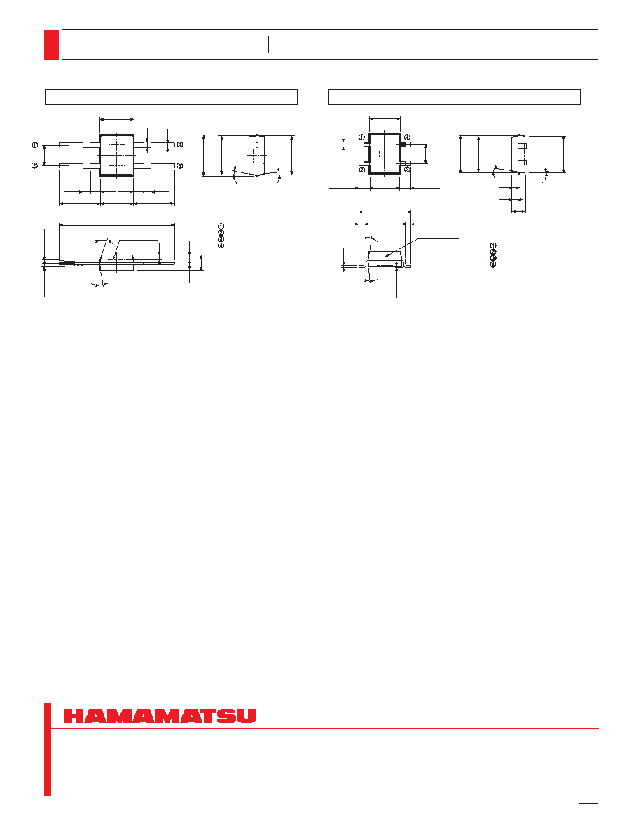
Si photodiodes
S5493-01, etc.
4
5.0
±
0.2
(Including
burr)
4.7
*
10°
4.8
*
5°
0.5
0.6
2.54
1.5 ± 0.4
1.8
0.8
10°
5°
7.0 ± 0.3
0.7 ± 0.3
0.25
0.1
±
0.1
Photosensitive
surface
4.0
*
4.1 ± 0.2
(Including burr)
Anode
Cathode
NC
Cathode
Chip position accuracy with
respect to the package
dimensions marked
*
X, Y ±0.2
θ ±2°
Lead surface finish: Silver plating
Packing: Stick (50 pcs/stick)
NC
Cathode
Anode
Cathode
4.6 ± 0.2
(Including burr)
4.5
*
5.0 ± 0.4
(1.0)
14.5 ± 0.3
(0.8)
0.7
0.5
5.6
±
0.2
(Including
burr)
0.3
Max.
0.3
Max.
5°
1.0
0.25
2.0
3°
5.4
*
10°
5.5
*
3°
2.54
(0.8)
0.7
Photosensitive
surface
Chip position accuracy with
respect to the package
dimensions marked
*
X, Y ±0.2
θ ±2°
Lead surface finish: Silver plating
Packing: Stick (50 pcs/stick)
S2833-01
S4011-04
KSPDA0123EB
KSPDA0163EB
相关PDF资料 |
PDF描述 |
|---|---|
| S42180H | SINGLE COLOR LED, NATURAL WHITE, 5.6 mm |
| S4282-11 | LOGIC OUTPUT PHOTO DETECTOR |
| S5107 | PIN PHOTO DIODE |
| S5531 | PIN PHOTO DIODE |
| S4753 | PIN PHOTO DIODE |
相关代理商/技术参数 |
参数描述 |
|---|---|
| S4011-46 | 制造商:Harwin 功能描述:Blade Terminal Tab 10.05mm 4.4mm Tin Reel |
| S4012 | 功能描述:SW TOGGLE SPDT 6A SOLDER LUG RoHS:是 类别:开关 >> 拨动开关 系列:S 标准包装:1 系列:A 电路:双刀双掷 开关功能:开-开-开 触点额定电压:6A @ 125VAC 触动器类型:扁平型 触动器长度:11.38mm 发光:不发光 安装类型:面板安装 端接类型:焊片 轴衬螺纹:1/4-40 包装:散装 |
| S-40-12 | 功能描述:线性和开关式电源 42W 12V 3.5A RoHS:否 制造商:TDK-Lambda 产品:Switching Supplies 开放式框架/封闭式:Enclosed 输出功率额定值:800 W 输入电压:85 VAC to 265 VAC 输出端数量:1 输出电压(通道 1):20 V 输出电流(通道 1):40 A 商用/医用: 输出电压(通道 2): 输出电流(通道 2): 安装风格:Rack 长度: 宽度: 高度: |
| S4012D | 制造商:LITTELFUSE 制造商全称:Littelfuse 功能描述:SCRs (1 A to 70 A) |
| S4012D56 | 制造商:LITTELFUSE 制造商全称:Littelfuse 功能描述:Teccor brand Thyristors 12 Amp Standard SCRs |
发布紧急采购,3分钟左右您将得到回复。