- 您现在的位置:买卖IC网 > PDF目录96808 > S7183 LINEAR OUTPUT PHOTO DETECTOR PDF资料下载
参数资料
| 型号: | S7183 |
| 元件分类: | 光电元器件 |
| 英文描述: | LINEAR OUTPUT PHOTO DETECTOR |
| 封装: | PLASTIC PACKAGE-2 |
| 文件页数: | 2/2页 |
| 文件大小: | 92K |
| 代理商: | S7183 |
HAMAMATSU PHOTONICS K.K., Solid State Division
1126-1 Ichino-cho, Higashi-ku, Hamamatsu City, 435-8558 Japan, Telephone: (81) 53-434-3311, Fax: (81) 53-434-5184, www.hamamatsu.com
U.S.A.: Hamamatsu Corporation: 360 Foothill Road, P.O.Box 6910, Bridgewater, N.J. 08807-0910, U.S.A., Telephone: (1) 908-231-0960, Fax: (1) 908-231-1218
Germany: Hamamatsu Photonics Deutschland GmbH: Arzbergerstr. 10, D-82211 Herrsching am Ammersee, Germany, Telephone: (49) 8152-375-0, Fax: (49) 8152-265-8
France: Hamamatsu Photonics France S.A.R.L.: 19, Rue du Saule Trapu, Parc du Moulin de Massy, 91882 Massy Cedex, France, Telephone: 33-(1) 69 53 71 00, Fax: 33-(1) 69 53 71 10
United Kingdom: Hamamatsu Photonics UK Limited: 2 Howard Court, 10 Tewin Road, Welwyn Garden City, Hertfordshire AL7 1BW, United Kingdom, Telephone: (44) 1707-294888, Fax: (44) 1707-325777
North Europe: Hamamatsu Photonics Norden AB: Smidesvgen 12, SE-171 41 Solna, Sweden, Telephone: (46) 8-509-031-00, Fax: (46) 8-509-031-01
Italy: Hamamatsu Photonics Italia S.R.L.: Strada della Moia, 1/E, 20020 Arese, (Milano), Italy, Telephone: (39) 02-935-81-733, Fax: (39) 02-935-81-741
Information furnished by HAMAMATSU is believed to be reliable. However, no responsibility is assumed for possible inaccuracies or omissions.
Specifications are subject to change without notice. No patent rights are granted to any of the circuits described herein.
Type numbers of products listed inthe specification sheets or supplied as samples may have a suffix "(X)" which means tentative specifications or a suffix "(Z)"
which means developmental specifications. 2009 Hamamatsu Photonics K.K.
Photo IC diode
S7183, S7184
Cat. No. KPIC1022E03
Aug. 2009 DN
0
200
WAVELENGTH (nm)
RELATIVE
SENSITIVITY
400
600
800
1000
1200
(Typ. Ta=25 C, VR=5 V)
0.2
0.4
0.6
0.8
1.0
0.1
0.3
0.5
0.7
0.9
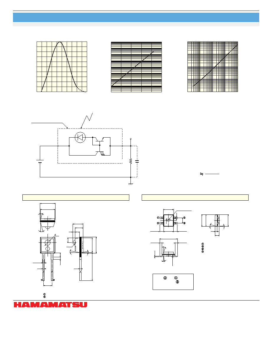
s Spectral response
KPICB0036EA
100 fA
-25
AMBIENT TEMPERATURE (C)
DARK
CURRENT
0
255075
100
(Typ. VR=5 V)
1 nA
100 pA
10 pA
1 pA
10 nA
100 nA
1
A
10
A
s Dark current vs. ambient
temperature
KPICB0042EA
0.01
100
LOAD RESISTANCE (
)
RISE/F
ALL
TIME
(ms)
1 k
10 k
100 k
1 M
(Typ. Ta=25 C, VR=5 V,
λ=560 nm, Vo=2.5 V)
1
0.1
10
100
s Rise/fall time vs. load resistance
KPICB0043EA
CATHODE
DRAWING WITHIN DASHED
LINE SHOWS SCHEMATIC
DIAGRAM OF PHOTO IC DIODE.
ANODE
REVERSE BIAS
POWER SUPPLY
LOAD CAPACITANCE
FOR
LOW-PASS FILTER CL
RL
LOAD RESISTANCE
s Operating circuit example
KPICC0018EA
The photodiode must be reverse-biased
so that a positive potential is applied to the
cathode.
To
eliminate
high-frequency
components, we recommend placing a
load capacitance CL in parallel with load
resistance RL as a low-pass filter.
s Dimensional outlines (unit: mm)
4.3 ± 0.3
(INCLUDING BURR)
4.15
3.0
2.4
R 0.9
0.45
0.6
10
5
10
5
0.45
2.54 ± 0.5
0.6 ± 0.3
(0.8)
(1.2)
1.43
4.43
15
MIN.
1.4
Tolerance unless otherwise
noted: ±0.2, ±2
Shaded area indicates burr.
Values in parentheses are not
guaranteed, but for reference.
1.7
(INCLUDING
B
URR)
4.6
+0.6 -0.3
CATHODE
ANODE
(SPECIFIED AT THE LEAD ROOT)
KPICA0017EB
KPICA0018EB
4.1 ± 0.2
(INCLUDING BURR)
4.0*
2.54
1.5 ± 0.4
0.6
0.47
5.0
±
0.2
(INCLUDING
BURR)
4.7*
10
4.8
5
1.8
0.8
7.0 ± 0.3
0.25
10
5
0.7 ± 0.3
0.1
±
0.1
CATHODE
(ANODE)
ANODE
(ANODE)
Tolerance unless otherwise
noted: ±0.1, ±2
Shaded area indicates burr.
Chip position accuracy with
respect to the package
dimensions marked *
X
≤±0.25, Y≤±0.25, G≤±2
CENTER OF
ACTIVE AREA
S7183
S7184
Pins
and
must be
connected to
on the
PC board.
Cut-off frequency fc
2
πCLRL
1
相关PDF资料 |
PDF描述 |
|---|---|
| S7184 | LINEAR OUTPUT PHOTO DETECTOR |
| S7379-01 | PIN PHOTO DIODE |
| S7600A | SERIAL COMM CONTROLLER, PQFP48 |
| S7720-PI | 8-BIT, 8.2 MHz, OTHER DSP, PDIP28 |
| S7727 | LOGIC OUTPUT PHOTO DETECTOR |
相关代理商/技术参数 |
参数描述 |
|---|---|
| S7184 | 制造商:HAMAMATSU 制造商全称:Hamamatsu Corporation 功能描述:Photo IC diode Linear current amplification of photodiode output |
| S-719 | 制造商:RAF Electronic Hardware 功能描述:SPRING, COMPRESSION, 7.5N, 19.1MM; Body Length:19.1mm; Compressed Length:10mm; Compression Load Max:7.5N; External Diameter:6.35mm; Wire Diameter:0.6mm ;RoHS Compliant: Yes |
| S7191-45R | 功能描述:RFI SHIELD FINGER AU 5MM SMD 制造商:harwin inc. 系列:- 零件状态:有效 形状:- 厚度 - 总:0.197"(5.00mm) 宽度:0.120"(3.00mm) 长度:0.181"(4.60mm) 粘合剂:- 温度范围:-4°F ~ 158°F(-20°C ~ 70°C) 标准包装:1 |
| S7199-01 | 制造商:HAMAMATSU 制造商全称:Hamamatsu Corporation 功能描述:CCD area image sensor Front-illuminated FFT-CCDs for X-ray imaging |
| S7199-01_11 | 制造商:HAMAMATSU 制造商全称:Hamamatsu Corporation 功能描述:CCD area image sensor Front-illuminated FFT-CCDs for X-ray imaging |
发布紧急采购,3分钟左右您将得到回复。