- 您现在的位置:买卖IC网 > PDF目录365442 > S71PL127J04BAW9Z0 (Spansion Inc.) Based MCPs PDF资料下载
参数资料
| 型号: | S71PL127J04BAW9Z0 |
| 厂商: | Spansion Inc. |
| 英文描述: | Based MCPs |
| 中文描述: | 基于MCP的 |
| 文件页数: | 15/24页 |
| 文件大小: | 296K |
| 代理商: | S71PL127J04BAW9Z0 |
March 17, 2006S71PL-J_00_B3
S71PL-J Based MCPs
13
A d v a n c e I n f o r m a t i o n
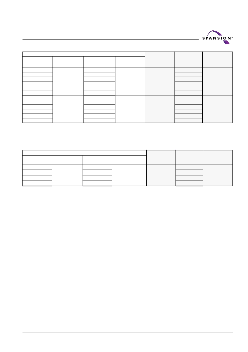
S71PL127J Valid Combinations
Speed Options
( ns)
( p) SRAM Type/
Access Time
( ns)
pSRAM7 / 70
pSRAM6 /70
pSRAM2 /70
pSRAM7 / 70
pSRAM6 / 70
pSRAM2 / 70
pSRAM7 / 70
pSRAM6 / 70
pSRAM2 /70
pSRAM7 / 70
pSRAM6 / 70
pSRAM2 / 70
Package Marking
Base Ordering
Part Number
Package &
Temperature
Package
Modifier/ Model
Number
9Z
9U
9B
9Z
9U
9B
9Z
9U
9B
9Z
9U
9B
Packing Type
S71PL127JB0
S71PL127JB0
S71PL127JC0
S71PL127JC0
S71PL127JC0
S71PL127JB0
S71PL127JB0
S71PL127JB0
S71PL127JC0
S71PL127JC0
S71PL127JC0
S71PL127JB0
BAW
0, 2, 3 (Note 1)
65
(Note 2)
BFW
0, 2, 3 (Note 1)
65
(Note 2)
S71PL254J Valid Combinations
Speed Options
( ns)
( p) SRAM
Type/ Access
Time ( ns)
Package
Marking
Base Ordering
Part Number
Package &
Temperature
Model Number
Packing Type
S71PL254JC0
BAW
TB
0, 2, 3 (Note1)
65
pSRAM2 / 70
(Note 2)
S71PL254JC0
TZ
pSRAM7 / 70
S71PL254JC0
BFW
TB
0, 2, 3 (Note1)
65
pSRAM2 / 70
(Note 2)
S71PL254JC0
TZ
pSRAM7 / 70
Notes:
1.
2.
Type 0 is standard. Specify other options as required.
BGA package marking omits leading “S” and packing type
designator from ordering part number.
Valid Combinations
Valid Combinations list configurations planned to be supported in vol-
ume for this device. Consult your local sales office to confirm avail-
ability of specific valid combinations and to check on newly released
combinations.
相关PDF资料 |
PDF描述 |
|---|---|
| S71PL127J04BAW9Z2 | Based MCPs |
| S71PL127J04BAW9Z3 | Based MCPs |
| S71PL127J04BAWTZ0 | Based MCPs |
| S71PL127J04BAWTZ2 | Based MCPs |
| S71PL127J04BAWTZ3 | Based MCPs |
相关代理商/技术参数 |
参数描述 |
|---|---|
| S71PL127J04BAW9Z2 | 制造商:SPANSION 制造商全称:SPANSION 功能描述:Based MCPs |
| S71PL127J04BAW9Z3 | 制造商:SPANSION 制造商全称:SPANSION 功能描述:Based MCPs |
| S71PL127J04BAWTZ0 | 制造商:SPANSION 制造商全称:SPANSION 功能描述:Based MCPs |
| S71PL127J04BAWTZ2 | 制造商:SPANSION 制造商全称:SPANSION 功能描述:Based MCPs |
| S71PL127J04BAWTZ3 | 制造商:SPANSION 制造商全称:SPANSION 功能描述:Based MCPs |
发布紧急采购,3分钟左右您将得到回复。