- 您现在的位置:买卖IC网 > PDF目录365464 > S72NS128PD0AJBLC3 (SPANSION LLC) MirrorBit Flash Memory and DRAM PDF资料下载
参数资料
| 型号: | S72NS128PD0AJBLC3 |
| 厂商: | SPANSION LLC |
| 元件分类: | 存储器 |
| 英文描述: | MirrorBit Flash Memory and DRAM |
| 中文描述: | SPECIALTY MEMORY CIRCUIT, PBGA133 |
| 封装: | 8 X 8 MM, 0.50 MM PITCH, LEAD FREE, FBGA-133 |
| 文件页数: | 8/14页 |
| 文件大小: | 335K |
| 代理商: | S72NS128PD0AJBLC3 |
6
S72NS-P Based MCPs/PoPs
S72NS-P_00_01 September 6, 2006
D a t a
S h e e t
( A d v a n c e
I n f o r m a t i o n )
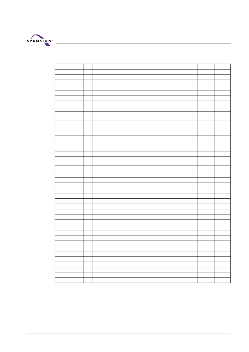
4.
Input/Output Descriptions
Signal
Description
Flash
DRAM
Amax – A16
=
Flash Address inputs
ADQ15 – ADQ0
=
Flash multiplexed Address and Data
F-CE#
=
Flash Chip-enable input. Asynchronous relative to CLK for Burst Mode
X
F-OE#
=
Flash Output Enable input. Asynchronous relative to CLK for Burst mode.
X
F-WE#
=
Flash Write Enable input
X
F-VCC
=
Flash device power supply (1.7 V to 1.95 V)
X
F-VCCQ
=
Flash Input/Output Buffer power supply
X
F-VSS
=
Flash Ground
X
F-RDY
=
Flash ready output. Indicates the status of the Burst read. V
OL
= data invalid. V
OH
= data valid.
X
F-CLK
=
Flash Clock. The first rising edge of CLK in conjunction with AVD# low latches the
address input and activates burst mode operation. After the initial word is output,
subsequent rising edges of CLK increment the internal address counter. CLK
should remain low during asynchronous access.
X
F-AVD#
=
Flash Address Valid input. Indicates to device that the valid address is present on
the address inputs. V
= for asynchronous mode, indicates valid address; for burst
mode, causes starting address to be latched on rising edge of CLK. V
IH
= device
ignores address inputs
X
F-RST#
=
Flash hardware reset input. V
IL
= device resets and returns to reading array data
X
F-WP#
=
Flash hardware write protect input. V
IL
= disables program and erase functions in
the four outermost sectors
X
F-ACC
=
Flash accelerated input. At V
, accelerates programming; automatically places
device in unlock bypass mode. At V
, disables all program and erase functions.
Should be at V
IH
for all other conditions.
DRAM Address inputs.
X
D-A12 – D-A0
=
X
D-DQ15 – D-DQ0
=
DRAM Data input/output
X
D-CLK
=
DRAM System Clock
X
D-CE#
=
DRAM Chip Select
X
D-CKE
=
DRAM Clock Enable
X
D-BA1 – BA0
=
DRAM Bank Select
X
D-RAS#
=
DRAM Row Address Strobe
X
D-CAS#
=
DRAM Column Address Strobe
X
D-UDQM – D-LDQM
=
DRAM Data Input Mask
X
D-WE#
=
DRAM Write Enable input
X
D-VSS
=
DRAM Ground
X
D-VSSQ
=
DRAM Input/Output Buffer ground
X
D-VCCQ
=
DRAM Input/Output Buffer power supply
X
D-VCC
=
DRAM device power supply
X
D-UDQS
=
DRAM Upper Data Strobe, output with read data and input with write data
X
D-LDQS
=
DRAM Lower Data Strobe, output with read data and input with write data
X
D-CLK#
=
DDR Clock for negative edge of CLK
X
RFU
=
Reserved for Future Use
NC
=
No Connect. Can be connected to ground or left floating.
DNU
=
Do Not Use. This signal must be left floating
相关PDF资料 |
PDF描述 |
|---|---|
| S72NS128PD0AJBLG | MirrorBit Flash Memory and DRAM |
| S72NS128PD0AJBLG0 | MirrorBit Flash Memory and DRAM |
| S72NS128PD0AJBLG2 | MirrorBit Flash Memory and DRAM |
| S72NS128PD0AJBLG3 | MirrorBit Flash Memory and DRAM |
| S72NS128PD0AJFGC0 | MirrorBit Flash Memory and DRAM |
相关代理商/技术参数 |
参数描述 |
|---|---|
| S72NS128PD0AJBLG | 制造商:SPANSION 制造商全称:SPANSION 功能描述:MirrorBit Flash Memory and DRAM |
| S72NS128PD0AJBLG0 | 制造商:SPANSION 制造商全称:SPANSION 功能描述:MirrorBit Flash Memory and DRAM |
| S72NS128PD0AJBLG2 | 制造商:SPANSION 制造商全称:SPANSION 功能描述:MirrorBit Flash Memory and DRAM |
| S72NS128PD0AJBLG3 | 制造商:SPANSION 制造商全称:SPANSION 功能描述:MirrorBit Flash Memory and DRAM |
| S72NS128PD0AJFGC0 | 制造商:SPANSION 制造商全称:SPANSION 功能描述:MirrorBit Flash Memory and DRAM |
发布紧急采购,3分钟左右您将得到回复。