- 您现在的位置:买卖IC网 > PDF目录96808 > S7600A SERIAL COMM CONTROLLER, PQFP48 PDF资料下载
参数资料
| 型号: | S7600A |
| 元件分类: | 微控制器/微处理器 |
| 英文描述: | SERIAL COMM CONTROLLER, PQFP48 |
| 封装: | 7 X 7 X 1.4 MM, LQFP-48 |
| 文件页数: | 5/9页 |
| 文件大小: | 64K |
| 代理商: | S7600A |
TCP/IP NETWORK PROTOCOL STACK LSI
S7600A Datasheet 1999/October
S-7600A
Seiko Instruments Inc.
5
68k Family MPU Mode
This mode can be selected by pulling the C86 input pin “H” and the PSX input pin “H”. In this mode, the address and data are
muxed into a single 8-bit bus. All cycles start by placing an address on the bus and setting the RS pin to “L”. In this mode WRITEX
signal works as read/write(R/WX) signal and READX is the enable (E) signal for 68k Family MPU interface. After the address cycle,
the MPU generates a read or writes strobe by setting the READX and WRITEX pins. The S-7600A MPU interface logic assert a
BUSYX signal low during data write and read phases. The MPU samples the BUSYX bit before starting a new cycle. The can
initiate a new cycle if the bit is “H”.
x80 Family MPU Mode
This mode is selected by pulling the C86 input pin “L” and the PSX input pin “H”. In this mode, the address and data are muxed
onto a single 8-bit bus. All cycles start with the address placed on the bus. This address is then latched internally on the rising edge
of WRITEX. The RS pin “L” indicates that the WRITEX strobe is for the address phase. In the next phase, data is either written or
read by generating WRITEX or READX strobe. The MPU interface logic will assert the BUSYX signal after READX or WRITEX
strobes are de-asserted.
The BUSYX signal is de-asserted after the S-7600A complete a read or writes operation. The MPU
samples the BUSYX bit before starting a new cycle. The MPU can initiate a new cycle after the BUSYX signal gets de-asserted.
Serial Interface
This mode is selected by pulling the PSX input pin “L”. In this mode Bit 6 of the Data Bus is used as the serial clock and bit 5 and
7 are used as Data Input and Data Output. Bit 0 to 4 are high impedance. By pulling WRITEX signal to “H” or “L”, the MPU performs
a read or write operation.
Interrupt
The interrupt signal outputs an active level while the interrupt flag is set in the interrupt register in the S-7600A’s interrupt register.
The interrupt signal returns to an inactive level if the flag clears.
The INT1 and INT2X can be Open Drain or CMOS output depending on the setting of INTCTL. The INT1 and INT2X outputs are
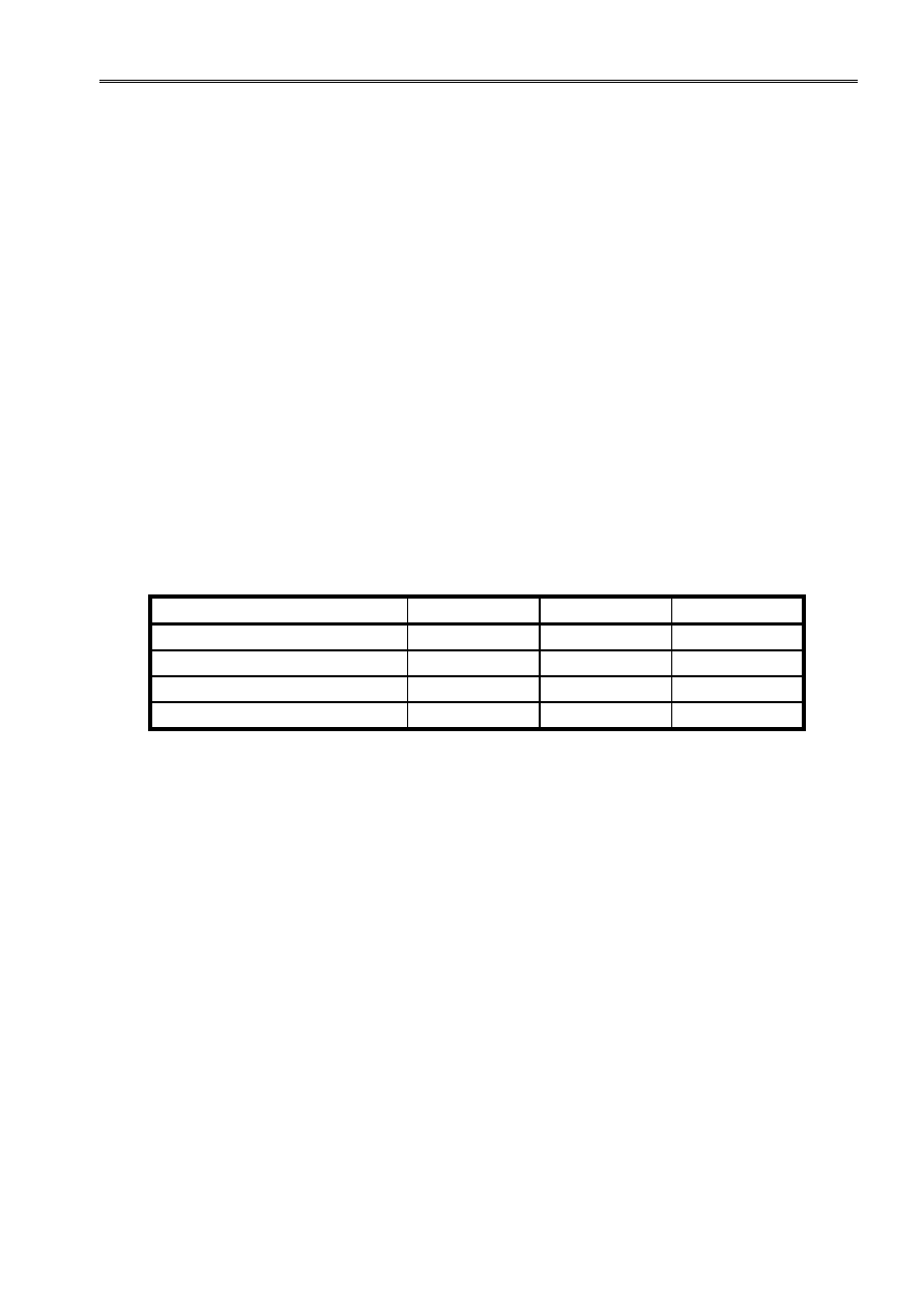
CMOS if INTCTL is “H” otherwise outputs are Open Drain. Table 7 defines the interrupt selection.
Table 7
Interrupt Selection
Interrupt flag
INTCTL
INT1
INT2X
Set
H
L
Set
L
H
L
Reset
H
L
H
Reset
L
Hi-Z
相关PDF资料 |
PDF描述 |
|---|---|
| S7720-PI | 8-BIT, 8.2 MHz, OTHER DSP, PDIP28 |
| S7727 | LOGIC OUTPUT PHOTO DETECTOR |
| S7747 | PIN PHOTO DIODE |
| S7848-01 | PHOTO DIODE |
| S7858 | LOGIC OUTPUT PHOTO DETECTOR |
相关代理商/技术参数 |
参数描述 |
|---|---|
| S-7600A | 功能描述:网络控制器与处理器 IC TCP/IP PROTOCOL STK RoHS:否 制造商:Micrel 产品:Controller Area Network (CAN) 收发器数量: 数据速率: 电源电流(最大值):595 mA 最大工作温度:+ 85 C 安装风格:SMD/SMT 封装 / 箱体:PBGA-400 封装:Tray |
| S760BK | 功能描述:直流电源连接器 LOCKING MINI PWR PLG WHITE 0.080" 2.0mm RoHS:否 制造商:Kycon 产品:Receptacles 触点内径: 触点外径: 中心脚长度: 电流额定值:7.5 A 电压额定值:20 V 安装角:Right 安装风格:Cable |
| S760BK-1MTR | 制造商:Switchcraft 功能描述:Locking 2.0mm DC Power Plug Cable 1m |
| S760K | 功能描述:直流电源连接器 DC PWR PLG 0.080" 1.7"L, BLK HAND. LCK RoHS:否 制造商:Kycon 产品:Receptacles 触点内径: 触点外径: 中心脚长度: 电流额定值:7.5 A 电压额定值:20 V 安装角:Right 安装风格:Cable |
| S760K | 制造商:Switchcraft 功能描述:JACK PLUG DC |
发布紧急采购,3分钟左右您将得到回复。