- 您现在的位置:买卖IC网 > PDF目录69327 > S80L188EB-16 (INTEL CORP) 16-BIT, 16 MHz, MICROPROCESSOR, PQFP80 PDF资料下载
参数资料
| 型号: | S80L188EB-16 |
| 厂商: | INTEL CORP |
| 元件分类: | 微控制器/微处理器 |
| 英文描述: | 16-BIT, 16 MHz, MICROPROCESSOR, PQFP80 |
| 封装: | QFP-80 |
| 文件页数: | 17/59页 |
| 文件大小: | 1928K |
| 代理商: | S80L188EB-16 |
第1页第2页第3页第4页第5页第6页第7页第8页第9页第10页第11页第12页第13页第14页第15页第16页当前第17页第18页第19页第20页第21页第22页第23页第24页第25页第26页第27页第28页第29页第30页第31页第32页第33页第34页第35页第36页第37页第38页第39页第40页第41页第42页第43页第44页第45页第46页第47页第48页第49页第50页第51页第52页第53页第54页第55页第56页第57页第58页第59页
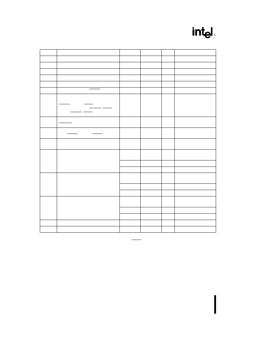
80C186EB80C188EB 80L186EB80L188EB
DC SPECIFICATIONS (80C186EB80C188EB)
Symbol
Parameter
Min
Max
Units
Notes
VCC
Supply Voltage
45
55
V
VIL
Input Low Voltage
b
05
03 VCC
V
VIH
Input High Voltage
07 VCC
VCC a 05
V
VOL
Output Low Voltage
045
V
IOL e 3 mA (Min)
VOH
Output High Voltage
VCC b 05
V
IOH eb2 mA (MIn)
VHYR
Input Hysterisis on RESIN
050
V
ILI1
Input Leakage Current for Pins
g
15
m
A0V s VIN s VCC
AD150 (AD70) READY HOLD
RESIN CLKIN TEST NMI INT40
T0IN T1IN RXD0 BCLK0 CTS0
RXD1 BCLK1 CTS1 P26 P27
ILI2
Input Leakage Current for Pins
g
0275
g
7mA
0V s VIN k VCC
ERROR PEREQ
ILI3
Input Leakage Current for Pins
b
0275
b
50
mA
VIN e 07 VCC (Note 1)
A19ONCE A1816 LOCK
ILO
Output Leakage Current
g
15
m
A
045 s VOUT s VCC
(Note 2)
ICC
Supply Current Cold (RESET)
80C186EB25
115
mA
(Notes 3 7)
80C186EB20
108
mA
(Note 3)
80C186EB13
73
mA
(Note 3)
IID
Supply Current Idle
80C186EB25
91
mA
(Notes 4 7)
80C186EB20
76
mA
(Note 4)
80C186EB13
48
mA
(Note 4)
IPD
Supply Current Powerdown
80C186EB25
100
m
A
(Notes 5 7)
80C186EB20
100
m
A
(Note 5)
80C186EB13
100
m
A
(Note 5)
CIN
Input Pin Capacitance
0
15
pF
TF e 1 MHz
COUT
Output Pin Capacitance
0
15
pF
TF e 1 MHz (Note 6)
NOTES
1 These pins have an internal pull-up device that is active while RESIN is low and ONCE Mode is not active Sourcing more
current than specified (on any of these pins) may invoke a factory test mode
2 Tested by outputs being floated by invoking ONCE Mode or by asserting HOLD
3 Measured with the device in RESET and at worst case frequency VCC and temperature with ALL outputs loaded as
specified in AC Test Conditions and all floating outputs driven to VCC or GND
4 Measured with the device in HALT (IDLE Mode active) and at worst case frequency VCC and temperature with ALL
outputs loaded as specified in AC Test Conditions and all floating outputs driven to VCC or GND
5 Measured with the device in HALT (Powerdown Mode active) and at worst case frequency VCC and temperature with
ALL
outputs loaded as specified in AC Test Conditions and all floating outputs driven to VCC or GND
6 Output Capacitance is the capacitive load of a floating output pin
7 Operating temperature for 25 MHz is 0 Cto70 C VCC e 50 g10%
24
相关PDF资料 |
PDF描述 |
|---|---|
| S80C186EB-25 | 16-BIT, 25 MHz, MICROPROCESSOR, PQFP80 |
| S80C186EB-13 | 16-BIT, 13 MHz, MICROPROCESSOR, PQFP80 |
| S80L188EB-13 | 16-BIT, 13 MHz, MICROPROCESSOR, PQFP80 |
| S80C196EA | 16-BIT, MICROCONTROLLER, PQFP16 |
| S80C652-2N40 | 8-BIT, 12 MHz, MICROCONTROLLER, PDIP40 |
相关代理商/技术参数 |
参数描述 |
|---|---|
| S80L188EB8 | 制造商:INTEL 制造商全称:Intel Corporation 功能描述:16-BIT HIGH-INTEGRATION EMBEDDED PROCESSORS |
| S80L188EC13 | 制造商:INTEL 制造商全称:Intel Corporation 功能描述:16-BIT HIGH-INTEGRATION EMBEDDED PROCESSORS |
| S80L188EC16 | 制造商:INTEL 制造商全称:Intel Corporation 功能描述:16-BIT HIGH-INTEGRATION EMBEDDED PROCESSORS |
| S80L188EC20 | 制造商:INTEL 制造商全称:Intel Corporation 功能描述:16-BIT HIGH-INTEGRATION EMBEDDED PROCESSORS |
| S80L188EC25 | 制造商:INTEL 制造商全称:Intel Corporation 功能描述:16-BIT HIGH-INTEGRATION EMBEDDED PROCESSORS |
发布紧急采购,3分钟左右您将得到回复。