- 您现在的位置:买卖IC网 > PDF目录96808 > S8550 AVALANCHE PHOTO DIODE PDF资料下载
参数资料
| 型号: | S8550 |
| 元件分类: | 光敏二极管 |
| 英文描述: | AVALANCHE PHOTO DIODE |
| 封装: | CERAMIC PACKAGE-34 |
| 文件页数: | 2/2页 |
| 文件大小: | 101K |
| 代理商: | S8550 |
HAMAMATSU PHOTONICS K.K., Solid State Division
1126-1 Ichino-cho, Higashi-ku, Hamamatsu City, 435-8558 Japan, Telephone: (81) 53-434-3311, Fax: (81) 53-434-5184, www.hamamatsu.com
U.S.A.: Hamamatsu Corporation: 360 Foothill Road, P.O.Box 6910, Bridgewater, N.J. 08807-0910, U.S.A., Telephone: (1) 908-231-0960, Fax: (1) 908-231-1218
Germany: Hamamatsu Photonics Deutschland GmbH: Arzbergerstr. 10, D-82211 Herrsching am Ammersee, Germany, Telephone: (49) 08152-3750, Fax: (49) 08152-2658
France: Hamamatsu Photonics France S.A.R.L.: 19, Rue du Saule Trapu, Parc du Moulin de Massy, 91882 Massy Cedex, France, Telephone: 33-(1) 69 53 71 00, Fax: 33-(1) 69 53 71 10
United Kingdom: Hamamatsu Photonics UK Limited: 2 Howard Court, 10 Tewin Road, Welwyn Garden City, Hertfordshire AL7 1BW, United Kingdom, Telephone: (44) 1707-294888, Fax: (44) 1707-325777
North Europe: Hamamatsu Photonics Norden AB: Smidesvgen 12, SE-171 41 Solna, Sweden, Telephone: (46) 8-509-031-00, Fax: (46) 8-509-031-01
Italy: Hamamatsu Photonics Italia S.R.L.: Strada della Moia, 1/E, 20020 Arese, (Milano), Italy, Telephone: (39) 02-935-81-733, Fax: (39) 02-935-81-741
Information furnished by HAMAMATSU is believed to be reliable. However, no responsibility is assumed for possible inaccuracies or omissions.
Specifications are subject to change without notice. No patent rights are granted to any of the circuits described herein. 2006 Hamamatsu Photonics K.K.
Si APD array
S8550
Cat. No. KAPD1009E02
Jun. 2006 DN
H4
H3
H2
H1
G4
G3
G2
G1
F4
F3
F2
F1
E4
E3
E2
E1
D4
D3
D2
D1
C4
C3
C2
C1
B4
B3
B2
B1
A4
A3
A2
A1
1.27
1.00
(0.5)
15.24
2.6
0.9
19.50
2.30
15.24
1.27
2.30
11.20
1.27
7.62
2.60
2.30
13 12 11 10 987654321
a
d
e
f
c
b
INDEX MARK
ARRAY 1
PHOTOSENSITIVE
SURFACE
ACTIVE AREA
1.6 × 1.6 (ANODE)
CATHODE 1: CATHODE OF ARRAY 1
CATHODE 2: CATHODE OF ARRAY 2
Pin No. Element No. Pin No. Element No. Pin No. Element No. Pin No. Element No.
1a
3a
5a
7a
9a
11a
13a
2b
4b
CATHODE 1
B1
C2
D2
E2
G1
H1
A2
C1
6b
8b
10b
12b
1c
3c
11c
13c
1d
D1
E1
F1
G2
A1
B2
F2
H2
A3
3d
11d
13d
2e
4e
6e
8e
10e
12e
C3
G3
H4
B3
C4
D4
E4
F4
H3
1f
3f
5f
7f
9f
11f
13f
A4
B4
D3
E3
F3
G4
CATHODE 2
ARRAY 2
0.45
200
400
600
800
1000
1200
0
40
20
60
80
100
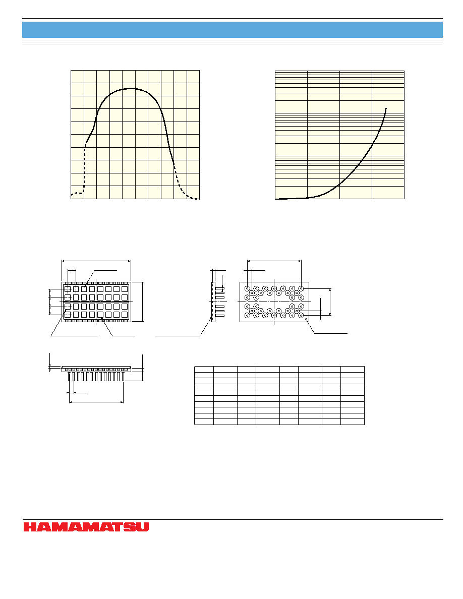
WAVELENGTH (nm)
QUANTUM
EFFICIENCY
(%)
(Typ. Ta=25 C)
s Quantum efficiency vs. wavelength
KAPDB0059EA
s Gain vs. reverse voltage
KAPDB0063EA
s Dimensional outline (unit: mm)
KAPDA0023EB
REVERSE VOLTAGE (V)
GAIN
100
0
1
10
1000
(Typ. Ta=25 C,
λ=420 nm)
100
200
300
400
2
相关PDF资料 |
PDF描述 |
|---|---|
| S8554 | PHOTO DIODE |
| S8594 | PIN PHOTO DIODE |
| S8627-01B | LOGIC OUTPUT PHOTO DETECTOR |
| S8673 | PHOTO DIODE |
| S8703 | PIN PHOTO DIODE |
相关代理商/技术参数 |
参数描述 |
|---|---|
| S-8550 | 制造商:SII 制造商全称:Seiko Instruments Inc 功能描述:STEP-DOWN, BUILT-IN FET, SYNCHRONOUS RECIFICATION, PWM CONTROL SWITCHING REGULATORS |
| S8550_09 | 制造商:UTC-IC 制造商全称:UTC-IC 功能描述:LOW VOLTAGE HIGH CURRENT SMALL SIGNAL PNP TRANSISTOR |
| S-8550AA-I8T1G | 制造商:Seiko Instruments Inc (SII) 功能描述:STEP DOWN SYNC 1.2MHZ PWM SWR |
| S-8550AA-I8T1U | 功能描述:IC REG BUCK ADJ 0.6A SNT-8A 制造商:ablic u.s.a. inc. 系列:- 包装:剪切带(CT) 零件状态:在售 功能:降压 输出配置:正 拓扑:降压 输出类型:可调式 输出数:1 电压 - 输入(最小值):2V 电压 - 输入(最大值):5.5V 电压 - 输出(最小值/固定):1.1V 电压 - 输出(最大值):4V 电流 - 输出:600mA 频率 - 开关:1.2MHz 同步整流器:是 工作温度:-40°C ~ 85°C(TA) 安装类型:表面贴装 封装/外壳:8-SMD,扁平引线 供应商器件封装:SNT-8A 标准包装:1 |
| S-8550AA-M5T1G | 功能描述:直流/直流开关调节器 Step Down Sync 1.2MHz PWM SWR RoHS:否 制造商:International Rectifier 最大输入电压:21 V 开关频率:1.5 MHz 输出电压:0.5 V to 0.86 V 输出电流:4 A 输出端数量: 最大工作温度: 安装风格:SMD/SMT 封装 / 箱体:PQFN 4 x 5 |
发布紧急采购,3分钟左右您将得到回复。