- 您现在的位置:买卖IC网 > PDF目录192312 > SB-36311CX-235N (DATA DEVICE CORP) SYNCHRO OR RESOLVER TO DIGITAL CONVERTER, XMA PDF资料下载
参数资料
| 型号: | SB-36311CX-235N |
| 厂商: | DATA DEVICE CORP |
| 元件分类: | 位置变换器 |
| 英文描述: | SYNCHRO OR RESOLVER TO DIGITAL CONVERTER, XMA |
| 文件页数: | 5/7页 |
| 文件大小: | 197K |
| 代理商: | SB-36311CX-235N |
5
Data Device Corporation
www.ddc-web.com
SB-36310CX
G-05/05-0
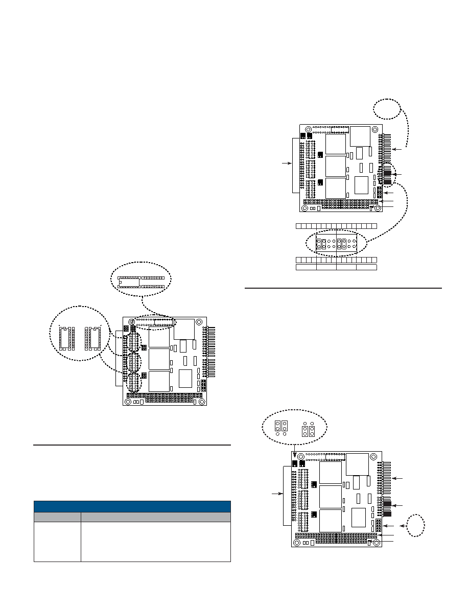
FIGURE 4. SYNCHRO/RESOLVER INPUT USING THIN-
FILM RESISTOR NETWORKS
RDC-19222S
Synchro
Resolver
Channel 4
Channels 1, 2, and 3
Synchro
Resolver
Ch.1
Ch. 2
Ch. 3
Ch. 4
SYNCHRO/RESOLVER INPUT SETTING
The input configuration for each channel on the SB-36310CX is
determined by the thin-film resistor network position on the
board. Each channel has two possible positions for the thin-film
resistor network to be installed on the board. When viewing the
card with the J1/P1, J2/P2 connectors facing down, the left hand
socket is for synchro input and the right hand socket is for
resolver input (refer to FIGURE 4).
NOTE:
Channels 1, 2, and 3 have two sockets offset by
0.1”, and channel 4 has two sockets in line.
The signal amplitude is determined by the type of thin-film resis-
tor network purchased for each channel. The DDC-49530 will
accept 11.8 VL-L, the DDC-49590 will accept 90 VL-L, and the
DDC-55688 will accept 2 V sin/cos inputs. For more information
about the DDC-49530 and the DDC-49590 please refer to the
Thin-Film Resistor Network data sheet. The DDC-55688 can
only be placed in the resolver socket.
NOTE:
Unused Channels do not require a thin-film resistor
network.
Viewing card with J1/P1, J2/P2 pointing down
REGISTER ADDRESSING
The SB-36310CX is addressed in typical Base Address and
Offset fashion. Each read/write register is 16 bits wide.
The Memory Map of the I/O registers is detailed in TABLE 4.
TABLE 4. SB-36310CX MEMORY MAP
HEX OFFSET
READ/WRITE
00
02
04
06
08
Channel Select and Inhibit (Read/Write)
Bandwidth and Resolution (Read/Write)
Status Register (Read Only)
8 Bit Digital I/O (Read/Write)
Angle Data (Read Only)
REFERENCE INPUT
An excitation or reference on the primary of the synchro or
resolver is also needed to demodulate the synchro/resolver
signals. The SB-36310CX has resistors that attenuate the
reference to a level that is acceptable for the RDC-19222
converter.
For a 2 Vrms to 28 Vrms reference the jumpers should be set for
a 26 V nominal reference. For a 10 Vrms to 130 Vrms reference
the jumpers should be set for a 115 V nominal reference. Refer
to FIGURE 6 to set the jumpers.
FIGURE 6. REFERENCE CONFIGURATION
BASE ADDRESS SETTING
The Base Address of the SB-36310CX is preset at the factory to
HEX address 0330h as shown in FIGURE 5. The user may
choose from 0000h to 0FF0h in 10 HEX increments.
FIGURE 5. ADDRESS DECODING
RDC-19222S
J3
J4
J5
J6
J1/P1
J2/P2
26V
115V
26V
(CH1)
(CH2)
(CH3)
(CH4)
8
7
6
5
4
3
2
1
A0
A15
0
1
0
1
0 0
0
LSB
MSB
1
8
3
0
3
0
Binary
Hex
J5
(viewed from
edge of card)
I/O Connector
8 Bit Input
8 Bit Output
RDC-19222S
J3
J4
J5
J6
J1/P1
J2/P2
26V
115V
26V
(CH1)
(CH2)
(CH3)
(CH4)
26 V
115 V
Viewing card with
J1/P1, J2/P2
pointing down.
Factory
Use
Only
相关PDF资料 |
PDF描述 |
|---|---|
| SB-36311CX-236N | SYNCHRO OR RESOLVER TO DIGITAL CONVERTER, XMA |
| SB-36311CX-246N | SYNCHRO OR RESOLVER TO DIGITAL CONVERTER, XMA |
| SB-36311CX-316 | SYNCHRO OR RESOLVER TO DIGITAL CONVERTER, XMA |
| SB-36311CX-325 | SYNCHRO OR RESOLVER TO DIGITAL CONVERTER, XMA |
| SB-36311CX-335 | SYNCHRO OR RESOLVER TO DIGITAL CONVERTER, XMA |
相关代理商/技术参数 |
参数描述 |
|---|---|
| SB36L-A | 制造商:GULFSEMI 制造商全称:Gulf Semiconductor 功能描述:SURFACE MOUNT SCHOTTKY BARRIER RECTIFIER VOLTAGE: 60V CURRENT: 3.0A |
| SB370 | 制造商:EIC 制造商全称:EIC discrete Semiconductors 功能描述:SCHOTTKY BARRIER RECTIFIER DIODES |
| SB370_08 | 制造商:DIODES 制造商全称:Diodes Incorporated 功能描述:3.0A SCHOTTKY BARRIER RECTIFIER |
| SB370-B | 制造商:DIODES 制造商全称:Diodes Incorporated 功能描述:3.0A SCHOTTKY BARRIER RECTIFIER |
| SB370S | 制造商:EIC 制造商全称:EIC discrete Semiconductors 功能描述:SCHOTTKY BARRIER RECTIFIER DIODES |
发布紧急采购,3分钟左右您将得到回复。