参数资料
| 型号: | SC28L91A1B,551 |
| 厂商: | NXP Semiconductors |
| 文件页数: | 29/30页 |
| 文件大小: | 0K |
| 描述: | IC UART SINGLE W/FIFO 44-PQFP |
| 产品培训模块: | Stand-Alone UARTs |
| 标准包装: | 96 |
| 系列: | IMPACT |
| 特点: | 故障启动位检测 |
| 通道数: | 1,UART |
| FIFO's: | 16 字节 |
| 电源电压: | 3.3V,5V |
| 带自动流量控制功能: | 是 |
| 带故障启动位检测功能: | 是 |
| 带调制解调器控制功能: | 是 |
| 带CMOS: | 是 |
| 安装类型: | 表面贴装 |
| 封装/外壳: | 44-QFP |
| 供应商设备封装: | 44-PQFP(10x10) |
| 包装: | 管件 |
| 产品目录页面: | 828 (CN2011-ZH PDF) |
| 其它名称: | 568-1187 935267419551 SC28L91A1B-S |
第1页第2页第3页第4页第5页第6页第7页第8页第9页第10页第11页第12页第13页第14页第15页第16页第17页第18页第19页第20页第21页第22页第23页第24页第25页第26页第27页第28页当前第29页第30页
Philips Semiconductors
Product data sheet
SC28L91
3.3 V or 5.0 V Universal Asynchronous
Receiver/Transmitter (UART)
2004 Oct 21
8
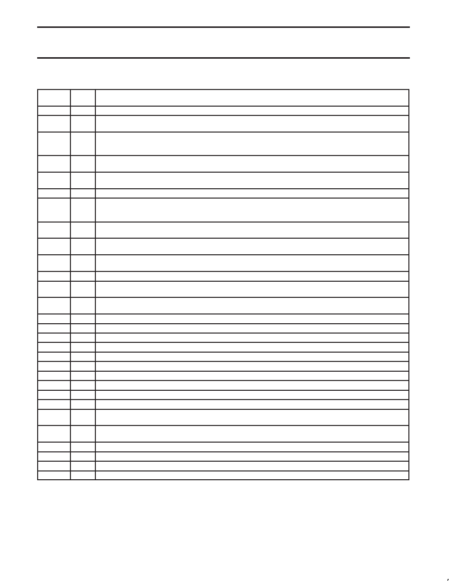
PIN CONFIGURATION FOR 80XXX BUS INTERFACE (INTEL)
Symbol
Pin
type
Name and function
I/M
I
Bus Configuration: When high or not connected configures the bus interface to the Conditions shown in this table.
D0–D7
I/O
Data Bus: Bi-directional 3-State data bus used to transfer commands, data and status between the UART and the
CPU. D0 is the least significant bit.
CEN
I
Chip Enable: Active-Low input signal. When Low, data transfers between the CPU and the UART are enabled on
D0–D7 as controlled by the WRN, RDN and A0–A3 inputs. When High, places the D0–D7 lines in the 3-State condi-
tion.
WRN
I
Write Strobe: When Low and CEN is also Low, the contents of the data bus is loaded into the addressed register. The
transfer occurs on the rising edge of the signal.
RDN
I
Read Strobe: When Low and CEN is also Low, causes the contents of the addressed register to be presented on the
data bus. The read cycle begins on the falling edge of RDN.
A0–A3
I
Address Inputs: Select the UART internal registers and ports for read/write operations.
RESET
I
Reset: A High level clears internal registers (SR, IMR, ISR, OPR, OPCR), puts OP0–OP7 in the High state, stops the
counter/timer, and puts the Channel in the inactive state, with the TxD outputs in the mark (High) state. Sets MR point-
er to MR1. See Figure 4
INTRN
O
Interrupt Request: Active-Low, open-drain, output which signals the CPU that one or more of the eight maskable in-
terrupting conditions are true. This pin requires a pull-up device.
X1/CLK
I
Crystal 1: Crystal or external clock input. A crystal or clock of the specified limits must be supplied at all times. When a
crystal is used, a capacitor must be connected from this pin to ground (see Figure 11).
X2
O
Crystal 2: Connection for other side of the crystal. When a crystal is used, a capacitor must be connected from this pin
to ground (see Figure 11). If X1/CLK is driven from an external source, this pin must be left open.
RxD
I
Receiver Serial Data Input: The least significant bit is received first. “Mark” is High; “space” is Low.
TxD
O
Transmitter Serial Data Output: The least significant bit is transmitted first. This output is held in the “mark” condition
when the transmitter is disabled, idle or operating in local loop back mode. “Mark” is High; “space” is Low.
OP0
O
Output 0: General-purpose output or request to send (RTSN, active-Low). Can be deactivated automatically on re-
ceive or transmit.
OP1
O
Output 1: General-purpose output.
OP2
O
Output 2: General-purpose output, or transmitter 1X or 16X clock output, or receiver 1X clock output.
OP3
O
Output 3: General-purpose output.
OP4
O
Output 4: General-purpose output or open-drain, active-Low, Rx interrupt ISR[1] output. DMA Control
OP5
O
Output 5: General-purpose output
OP6
O
Output 6: General-purpose output or open-drain, active-Low, Tx interrupt ISR[0] output. DMA Control
OP7
O
Output 7: General-purpose output.
IP0
I
Input 0: General-purpose input or clear to send active-Low input (CTSN). Has Change of State Dector.
IP1
I
Input 1: General-purpose input. Has Change of State Dector.
IP2
I
Input 2: General-purpose input or counter/timer external clock input. Has Change of State Dector.
IP3
I
Input 3: General-purpose input or transmitter external clock input (TxC). When the external clock is used by the trans-
mitter, the transmitted data is clocked on the falling edge of the clock. Has Change of State Dector.
IP4
I
Input 4: General-purpose input or receiver external clock input (RxC). When the external clock is used by the receiver,
the received data is sampled on the rising edge of the clock.
IP5
I
Input 5: General-purpose input
IP6
I
Input 6: General-purpose input
VCC
Pwr
Power Supply: +3.3 V or +5 V supply input
± 10 %
GND
Pwr
Ground
相关PDF资料 |
PDF描述 |
|---|---|
| SC28L91A1B,528 | IC UART SINGLE W/FIFO 44PQFP |
| SC28L91A1A,529 | IC UART SINGLE W/FIFO 44-PLCC |
| SCC68692C1A44,512 | IC UART DUAL 44-PLCC |
| SCC68692C1A44,518 | IC DUART 44PLCC |
| ATMEGA164PA-AUR | MCU AVR 16KB FLASH 20MHZ 44TQFP |
相关代理商/技术参数 |
参数描述 |
|---|---|
| SC28L91A1B-S | 功能描述:UART 接口集成电路 UART SINGLE W/FIFO RoHS:否 制造商:Texas Instruments 通道数量:2 数据速率:3 Mbps 电源电压-最大:3.6 V 电源电压-最小:2.7 V 电源电流:20 mA 最大工作温度:+ 85 C 最小工作温度:- 40 C 封装 / 箱体:LQFP-48 封装:Reel |
| SC28L91A1B-T | 功能描述:UART 接口集成电路 3V-5V 1CH UART INTEL/MOT INTRF RoHS:否 制造商:Texas Instruments 通道数量:2 数据速率:3 Mbps 电源电压-最大:3.6 V 电源电压-最小:2.7 V 电源电流:20 mA 最大工作温度:+ 85 C 最小工作温度:- 40 C 封装 / 箱体:LQFP-48 封装:Reel |
| SC28L92 | 制造商:PHILIPS 制造商全称:NXP Semiconductors 功能描述:3.3V-5.0V Dual Universal Asynchronous Receiver/Transmitter DUART |
| SC28L92A1A | 制造商:NXP Semiconductors 功能描述:UART DUAL 3.3V OR 5V SMD 28L92 |
| SC28L92A1A,512 | 功能描述:UART 接口集成电路 3V-5V 2CH UART INTEL/MOT INTRF RoHS:否 制造商:Texas Instruments 通道数量:2 数据速率:3 Mbps 电源电压-最大:3.6 V 电源电压-最小:2.7 V 电源电流:20 mA 最大工作温度:+ 85 C 最小工作温度:- 40 C 封装 / 箱体:LQFP-48 封装:Reel |
发布紧急采购,3分钟左右您将得到回复。