- 您现在的位置:买卖IC网 > PDF目录299883 > SC804 (Semtech Corporation) Fully Integrated Lithium-Ion Battery Charger System with Timer PDF资料下载
参数资料
| 型号: | SC804 |
| 厂商: | Semtech Corporation |
| 英文描述: | Fully Integrated Lithium-Ion Battery Charger System with Timer |
| 中文描述: | 完全集成的锂离子电池充电器系统的计时器 |
| 文件页数: | 5/21页 |
| 文件大小: | 548K |
| 代理商: | SC804 |
13
2007 Semtech Corp.
www.semtech.com
SC804
PRELIMINARY
POWER MANAGEMENT
current and the charge path resistance from VOUT to the
Kelvin sense point should not exceed 150mV to ensure
normal mode operation.
The SC804 Adjust Mode schematic is shown in Figures 3A
and 3B. Referring to these schematics, the equation for
setting the output voltage is:
The capacitor C3 across R8 in the feedback network
introduces zero-pole frequency compensation for stability.
Place the zero according to the following equation to
ensure stability:
NOTE: When using Adjust Mode to program a CV regulation
voltage greater than V
CV, care must be taken when CC
charging with a charging adapter operating in current
limit.
Adapter current-limited operation occurs when
the adapter current limit is less than the programmed
SC804 fast charge current, such that the adapter voltage
is pulled down to V
VOUT plus the SC804 dropout voltage. A
low adapter current limit multiplied by the low minimum
path resistance of the main pass transistor and current
sense resistor (as low as 290m
Ω total at extremely low
temperature) can result in a voltage drop from VCC to
VOUT of less than 150mV if the Adjust Mode CV regulation
voltage is programmed above V
CV + 50mV. If VVCC - VVOUT <
150mV, Adjust Mode may not operate correctly. Adjust
Mode will operate correctly whenever the programmed
VOUT CV voltage is less than V
CV + 50mV, regardless of the
adapter current limit, because the regulated minimum
dropout voltage is always greater than 150mV in this
case. It will also operate correctly with an adapter current
limit greater than 550 mA, regardless of the programmed
output voltage, because the I-R dropout voltage will
exceed 150mV at even the lowest specied operating
temperature. Normal mode (that is, not Adjust Mode) has
a regulated minimum dropout voltage of approximately
200mV, which is constant for any V
VOUT, and so operates
correctly for any adapter current limit.
Over current and Max Temperature Protection
Over current protection is inherent in all modes of
R11 × C3 =
1
2 × 100kHz
Applications Information (Cont.)
VOUT = V
BSEN-ADJ_Typ ×
(1 + R11 )
R12
operation. When the device is in charge mode the output
is current-limited to either the pre-charge current limit
value or the fast charge current limit value depending on
the voltage at the output. Max die temperature protection
is also included. This feature allows the SC804 to operate
with maximum power dissipation by disabling the output
current when the die temperature reaches the maximum
operating temperature. The result is that the SC804 will
operate as a pulse charger in extreme power dissipation
applications, delivering the maximum allowable output
current while regulating the internal die temperature to
a safe level.
Indicator Flags
There are four indicator outputs/LED drivers on the SC804:
CPB (Charger Present), CHRGB (Charge Active), OVPB
(Over Voltage Fault), and FLTB (Fault). These outputs are
all active-low, open drain NMOS drivers capable of sinking
up to 10mA. The following table denes each indicator’s
output state.
The CPB output can be used as a VCC-present indicator.
Regardless of the state of NTC, the CPB output reects
the VCC voltage. When V
VCC is between the UVLO and OVP
thresholds the CPB output is low. If V
VCC is outside these
limits this output is high impedance.
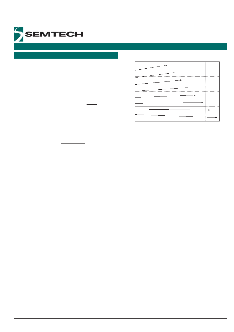
3.2
3.4
3.6
3.8
4
4.2
4.4
0.2
0.4
0.6
0.8
Output voltage, V
Mi
ni
mum
dr
opout
v
ol
tage,
V
Figure 4 - Adjust Mode Minimum Dropout Voltage
The actual dropout voltage is the greater of the Minimum Dropout
Voltage at various programmed V
CV and instantaneous VOUT
voltages (shown here, with several programmed V
CV voltages
indicated in the gure by ‘o’), and the IR drop due to the product
of IOUT and R
DS-ON (not shown here).
Adjust mode operation is
ensured for any IOUT current at programmed V
CV voltages up to
approximately 4.25V.
相关PDF资料 |
PDF描述 |
|---|---|
| SC805EVB | Miniature Integrated High Current Lithium-Ion Battery Charger |
| SC805IMLTRT | Miniature Integrated High Current Lithium-Ion Battery Charger |
| SC805 | Miniature Integrated High Current Lithium-Ion Battery Charger |
| SC806 | Miniature High Current Lithium-Ion Battery Charger |
| SCD25-590-318-15 | 50 CONTACT(S), MALE, STRAIGHT BOARD STACKING CONNECTOR, SOLDER |
相关代理商/技术参数 |
参数描述 |
|---|---|
| SC804A | 制造商:SEMTECH 制造商全称:Semtech Corporation 功能描述:Fully Integrated 4.4V Lithium-Ion Battery Charger System with Timer |
| SC804AMLTRT | 功能描述:IC LI-ION BATT CHARGER 16-MLPQ RoHS:是 类别:集成电路 (IC) >> PMIC - 电池管理 系列:- 标准包装:1 系列:- 功能:充电管理 电池化学:锂离子(Li-Ion)、锂聚合物(Li-Pol) 电源电压:3.75 V ~ 6 V 工作温度:-40°C ~ 85°C 安装类型:表面贴装 封装/外壳:SC-74A,SOT-753 供应商设备封装:SOT-23-5 包装:剪切带 (CT) 产品目录页面:669 (CN2011-ZH PDF) 其它名称:MCP73831T-2ACI/OTCT |
| SC804EVB | 制造商:SEMTECH 制造商全称:Semtech Corporation 功能描述:Fully Integrated 4.4V Lithium-Ion Battery Charger System with Timer |
| SC804IML.TRT | 功能描述:IC LI-ION BATTERY CHRGR 16MLPQ RoHS:是 类别:集成电路 (IC) >> PMIC - 电池管理 系列:- 标准包装:1 系列:- 功能:充电管理 电池化学:锂离子(Li-Ion)、锂聚合物(Li-Pol) 电源电压:3.75 V ~ 6 V 工作温度:-40°C ~ 85°C 安装类型:表面贴装 封装/外壳:SC-74A,SOT-753 供应商设备封装:SOT-23-5 包装:剪切带 (CT) 产品目录页面:669 (CN2011-ZH PDF) 其它名称:MCP73831T-2ACI/OTCT |
| SC804IMLTRT | 制造商:Semtech Corporation 功能描述:Battery Charger Li-Ion 1500mA 4.2V 16-Pin MLPQ EP T/R |
发布紧急采购,3分钟左右您将得到回复。