- 您现在的位置:买卖IC网 > PDF目录85287 > SCD03PAR LINEAR OPTICAL POSITION ENCODER PDF资料下载
参数资料
| 型号: | SCD03PAR |
| 元件分类: | 编、解码器及复用、解复用 |
| 英文描述: | LINEAR OPTICAL POSITION ENCODER |
| 文件页数: | 1/1页 |
| 文件大小: | 46K |
| 代理商: | SCD03PAR |
REV.
SCD-XX-PAR
A
Pin# 1
+15V
2
-15V
3
Output
40V
5
Input (+)
6
Output (-)
Model
A
B
SCD03PAR
0.7
1.2
SCD05PAR
1.0
1.5
SCD10PAR
1.2
1.7
SCD15PAR
1.5
2.0
SCD20PAR
1.8
2.3
Mounting Hole Dimensions
Pin Assignments
SPECIFICATIONS
(Vcc = ±15v, RL = 10k
, Ta = 25°C)
Model
SCD03PAR SCD05PAR SCD10PAR SCD15PAR SCD20PAR
Rated Current
±3A
±5A
±10A
±15A
±20A
Linearity Range
±9A
±10A
±20A
±30A
±40A
Output Voltage
4V ±1% @ Rated Current
Zero Current Offset Voltage
0V ±30mV max. (after demagnetization)
Output Voltage Linearity
± 0.5 % @ rated current
Supply Voltage
±15V ±5%
Max Current Consumption
±25mA max.
Response
3 S typ. @ 50 Amp/Turns/S
Output V Temp Char
± 0.1%/°C max. @ rated current
Zero Current Offset V Temp Char
± 1.5mV/°C max.
Hysteresis
15mV max. @ rated current to 0A
Primary Overcurrent
10X rated current, 50 mS, no damage
Withstand Voltage
2000 VAC, 50/60Hz, 1 minute between primary coil & terminal*
Insulation Resistance
500 VDC between primary coil & terminal
Operating Temp
-10° to 75° C
Storage Temp
-15 to 85°C
* "-S" model available with 4500VAC, 50/60Hz, 1 minute between primary coil & terminal.
PART NO.
DRAWN BY
UPDATED
CHECKED
RELEASED
Ordering Information
SCD
PAR
Current Rating:
03:
3A
05:
5A
10: 10A
15: 15A
20: 20A
Input Current Polarity:
N:
+(DC only)
R:
± (bipolar)
Input Voltage:
A: ±15VDC
B: ±12VDC
S: +12VDC
T:
±5VDC
CUI Stack, Inc.
9615 SW Allen Blvd.
Beaverton, OR
97005
Tel: 503/643-4899 FAX: 503/643-6129
6
5
4
3
2
1
B
+0.1
-0.0
+0.1
-0.0
0.80
0.50
5.0 ±1.0
4.0 ±1.0
2.54 ±0.1
7.62 ±0.2
10.0 ±0.1
MOUNTING FOOTPRINT
(Viewed from mounting side)
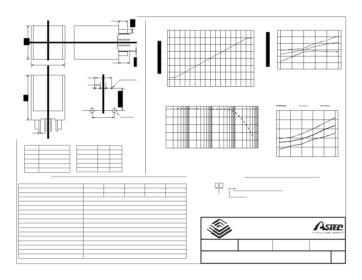
15
-20
-40
-20
0
20
40
60
TEMPERATURE (°C)
80
-60
0
20
40
60
Offset Voltage vs Temperature
4.00
3.90
-20
0
20
40
60
OUTPUT
VOLTAGE
(V)
TEMPERATURE (C)
80
3.95
4.05
4.10
4.15
MIN
MAX
AVG
Output Voltage vs Temperature
80
70
OUTPUT
SIGNAL
ATTEN
%
INPUT CURRENT FREQUENCY
100kHz
90
100
10kHz
1kHz
100Hz
10Hz
Signal Attenuation vs Input Current Frequency
-20
-40
-30
-20
-10
0
INPUT CURRENT (A)
10
20
30
40
-10
0
10
20
Output Voltage vs Input Current
相关PDF资料 |
PDF描述 |
|---|---|
| SF4-PG-2 | SINGLE COLOR LED ARRAY, PURE GREEN, 2.25 mm |
| S4100TY3-12V/30-P | SINGLE COLOR DISPLAY CLUSTER, YELLOW, 25.4 mm |
| S206CR7-28VAC-BP | SINGLE COLOR DISPLAY CLUSTER, RED, 5 mm |
| S206CR7-6VAC-P | SINGLE COLOR DISPLAY CLUSTER, RED, 5 mm |
| SLR-342VCTC7P | T-1 SINGLE COLOR LED, RED, 3.1 mm |
相关代理商/技术参数 |
参数描述 |
|---|---|
| SCD03PSN | 功能描述:SENSOR CURRENT 3A 12V UNI MOD RoHS:是 类别:传感器,转换器 >> 电流 系列:SCD 标准包装:10 系列:* |
| SCD03PSR | 功能描述:SENSOR CURRENT 3A 12V BI MOD RoHS:是 类别:传感器,转换器 >> 电流 系列:SCD 标准包装:10 系列:* |
| SCD03PUN | 功能描述:SENSOR CURRENT 3A 5V UNI MOD RoHS:是 类别:传感器,转换器 >> 电流 系列:SCD 标准包装:10 系列:* |
| SCD03PUR | 功能描述:SENSOR CURRENT 3A 5V BI MOD RoHS:是 类别:传感器,转换器 >> 电流 系列:SCD 标准包装:10 系列:* |
| SCD0403T-100M-N | 制造商:Yageo Corporation 功能描述: |
发布紧急采购,3分钟左右您将得到回复。