- 您现在的位置:买卖IC网 > PDF目录40160 > SFC05-4.WMT 300 W, UNIDIRECTIONAL, 4 ELEMENT, SILICON, TVS DIODE, MO-211BB PDF资料下载
参数资料
| 型号: | SFC05-4.WMT |
| 元件分类: | TVS二极管 - 瞬态电压抑制 |
| 英文描述: | 300 W, UNIDIRECTIONAL, 4 ELEMENT, SILICON, TVS DIODE, MO-211BB |
| 封装: | FLIP CHIP, MO-211, CSP-6 |
| 文件页数: | 5/8页 |
| 文件大小: | 218K |
| 代理商: | SFC05-4.WMT |
5
2004 Semtech Corp.
www.semtech.com
PRELIMINARY
PROTECTION PRODUCTS
SFC05-4
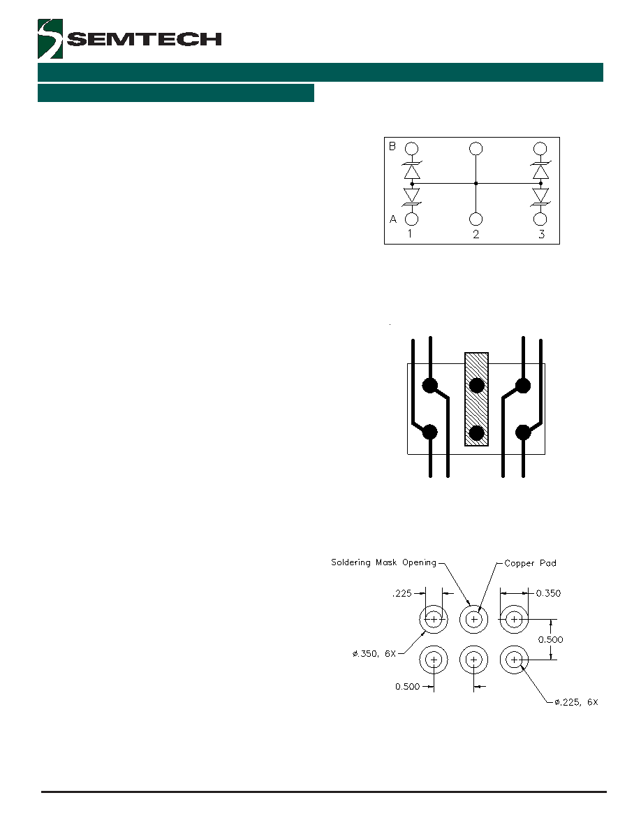
Device Connection Options
The SFC05-4 has solder bumps located in a 3 x 2
matrix layout on the active side of the device. The
bumps are designated by the numbers 1 - 3 along the
horizontal axis and letters A - B along the vertical axis.
The lines to be protected are connected at bumps A1,
B1, A3, and B3. Bumps A2 and B2 are connected to
ground. All path lengths should be kept as short as
possible to minimize the effects of parasitic inductance
in the board traces.
Flip Chip TVS
Flip chip TVS devices are wafer level chip scale pack-
ages. They eliminate external plastic packages and
leads and thus result in a significant board space
savings. Manufacturing costs are minimized since they
do not require an intermediate level interconnect or
interposer layer for reliable operation. Their compatibil-
ity with current pick and place equipment further
reduces manufacturing costs. Certain precautions and
design considerations have to be observed, however,
for maximum solder joint reliability. These include
solder pad definition, board finish, and assembly
parameters.
Printed Circuit Board Mounting
Non-solder mask defined (NSMD) land patterns are
recommended for mounting the SFC05-4. Solder
mask defined (SMD) pads produce stress points near
the solder mask on the PCB side that can result in
solder joint cracking when exposed to extreme fatigue
conditions. The recommended pad size is 0.225 ±
0.010 mm with a solder mask opening of 0.350 ±
0.025 mm.
Grid Courtyard
The recommended grid placement courtyard is 1.3 x
1.8 mm. The grid courtyard is intended to encompass
the land pattern and the component body that is
centered in the land pattern. When placing parts on a
PCB, the highest recommended density is when one
courtyard touches another.
Applications Information
Device Schematic and Pin Configuration
Layout Example
NSMD Package Footprint
To Protected IC
To Connector
Ground
相关PDF资料 |
PDF描述 |
|---|---|
| SFC05-5-T710-2 | 250 W, UNIDIRECTIONAL, 5 ELEMENT, SILICON, TVS DIODE |
| SFC05-5.WMT | 200 W, UNIDIRECTIONAL, 5 ELEMENT, SILICON, TVS DIODE, MO-211BB |
| SFF1605G | 16 A, 300 V, SILICON, RECTIFIER DIODE, TO-220AB |
| SFF1608G | 16 A, 600 V, SILICON, RECTIFIER DIODE, TO-220AB |
| SFF1606G | 16 A, 400 V, SILICON, RECTIFIER DIODE, TO-220AB |
相关代理商/技术参数 |
参数描述 |
|---|---|
| SFC05-5 | 制造商:PROTEC 制造商全称:Protek Devices 功能描述:FLIP CHIP ARRAY |
| SFC05-5.TC | 制造商:Semtech Corporation 功能描述:CHIPCLAMP FLIP CHIP TVS DIODE ARRAY |
| SFC05-5.WCT | 制造商:Semtech Corporation 功能描述:Diode |
| SFC05-5_07 | 制造商:PROTEC 制造商全称:Protek Devices 功能描述:FLIP CHIP ARRAY |
| SFC05-5_10 | 制造商:PROTEC 制造商全称:Protek Devices 功能描述:250w flip chip tvs array |
发布紧急采购,3分钟左右您将得到回复。