- 您现在的位置:买卖IC网 > PDF目录21886 > SFCF2048H1BK1TO-I-DT-553-SMA (Swissbit NA Inc)FLASH SLC UDMA/MDMA/PIO 2G PDF资料下载
参数资料
| 型号: | SFCF2048H1BK1TO-I-DT-553-SMA |
| 厂商: | Swissbit NA Inc |
| 文件页数: | 52/99页 |
| 文件大小: | 0K |
| 描述: | FLASH SLC UDMA/MDMA/PIO 2G |
| 视频文件: | Swissbit Manufacturing Overview |
| RoHS指令信息: | Environment Protection Declaration |
| 标准包装: | 20 |
| 系列: | C-300 |
| 存储容量: | 2GB |
| 存储器类型: | CompactFlash? |
| 其它名称: | 1052-1009 |
第1页第2页第3页第4页第5页第6页第7页第8页第9页第10页第11页第12页第13页第14页第15页第16页第17页第18页第19页第20页第21页第22页第23页第24页第25页第26页第27页第28页第29页第30页第31页第32页第33页第34页第35页第36页第37页第38页第39页第40页第41页第42页第43页第44页第45页第46页第47页第48页第49页第50页第51页当前第52页第53页第54页第55页第56页第57页第58页第59页第60页第61页第62页第63页第64页第65页第66页第67页第68页第69页第70页第71页第72页第73页第74页第75页第76页第77页第78页第79页第80页第81页第82页第83页第84页第85页第86页第87页第88页第89页第90页第91页第92页第93页第94页第95页第96页第97页第98页第99页
�� �
�
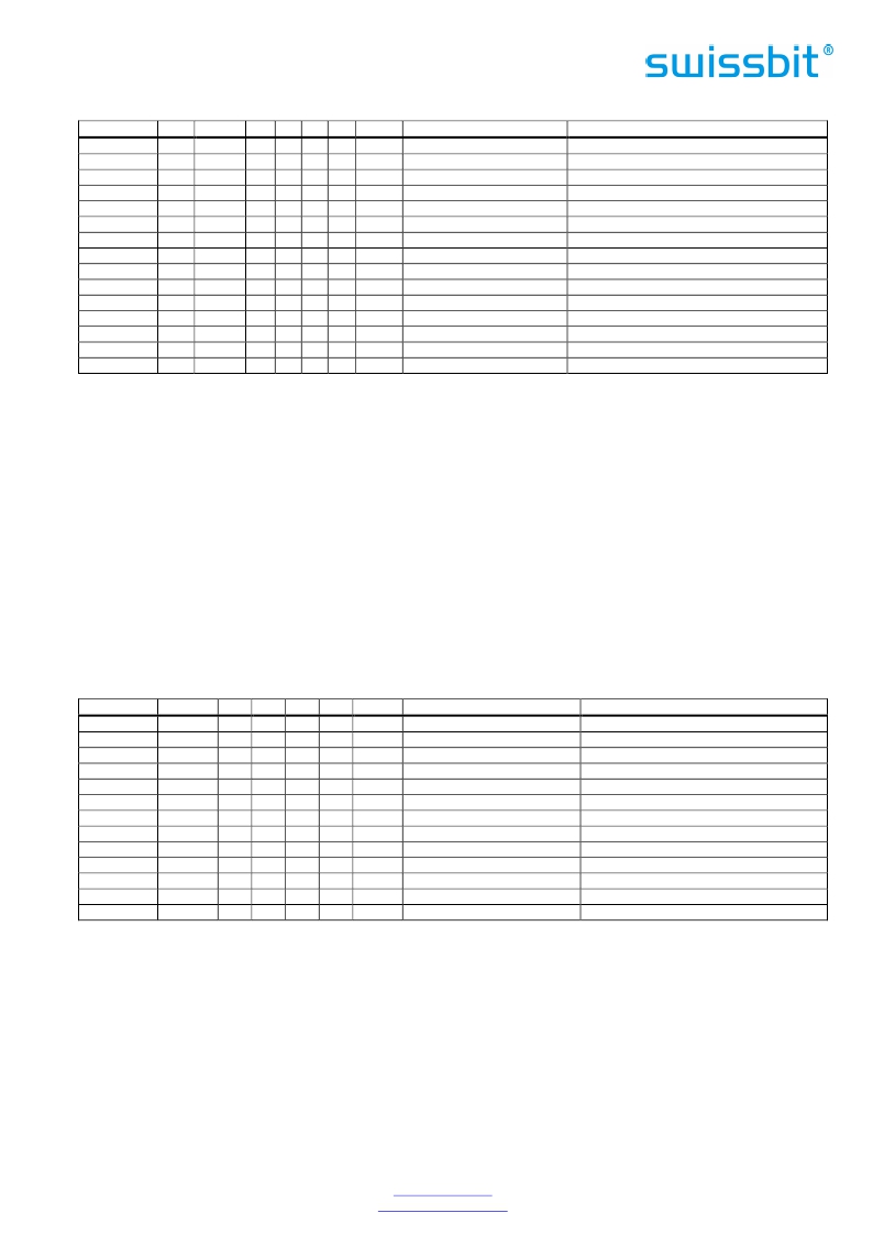
�Table� 44:� Memory� Mapped� Decoding�
�-� REG�
�A10� A9 to A4�
�A3�
�A2�
�A1�
�A0�
�Offset�
�-� OE=0�
�-� WE=0�
�1�
�1�
�1�
�1�
�1�
�1�
�1�
�1�
�1�
�1�
�1�
�1�
�1�
�1�
�1�
�0�
�0�
�0�
�0�
�0�
�0�
�0�
�0�
�0�
�0�
�0�
�0�
�0�
�1�
�1�
�X�
�X�
�X�
�X�
�X�
�X�
�X�
�X�
�X�
�X�
�X�
�X�
�X�
�X�
�X�
�0�
�0�
�0�
�0�
�0�
�0�
�0�
�0�
�1�
�1�
�1�
�1�
�1�
�X�
�X�
�0�
�0�
�0�
�0�
�1�
�1�
�1�
�1�
�0�
�0�
�1�
�1�
�1�
�X�
�X�
�0�
�0�
�1�
�1�
�0�
�0�
�1�
�1�
�0�
�0�
�0�
�1�
�1�
�X�
�X�
�0�
�1�
�0�
�1�
�0�
�1�
�0�
�1�
�0�
�1�
�1�
�0�
�1�
�0�
�1�
�0h�
�1h�
�2h�
�3h�
�4h�
�5h�
�6h�
�7h�
�8h�
�9h�
�Dh�
�Eh�
�Fh�
�8h�
�9h�
�Even� Data� Register�
�Error� Register�
�Sector� Count� Register�
�Sector� Number� Register�
�Cylinder� Low� Register�
�Cylinder� High� Register�
�Select� Card/Head� Register�
�Status� Register�
�Dup.� Even� Data� Register�
�Dup.� Odd� Data� Register�
�Dup.� Error� Register�
�Alternate� Status� Register�
�Drive� Address� Register�
�Even� Data� Register�
�Odd� Data� Register�
�Even� Data� Register�
�Feature� Register�
�Sector� Count� Register�
�Sector� Number� Register�
�Cylinder� Low� Register�
�Cylinder� High� Register�
�Select� Card/Head� Register�
�Command� Register�
�Dup.� Even� Data� Register�
�Dup.� Odd� Data� Register�
�Dup.� Feature� Register�
�Device� Control� Register�
�Reserved�
�Even� Data� Register�
�Odd� Data� Register�
�8.3� Contiguous� I/O� Mapped� Addressing�
�When� the� system� decodes� a� contiguous� block� of� I/O� registers� to� select� the� Card,� the� registers� are� accessed� in� the�
��As� for� the� Memory� Mapped� Addressing,� register� 0� is� accessed� with� –� CE1� Low� and� –CE2� Low� (and� A0� don’t� Care)� as� a�
�Word� register� on� the� combined� Odd� and� Even� Data� Bus� (D15� to� D0).� This� register� may� also� be� accessed� with� –� CE1�
�Low� and� –� CE2� High,� by� a� pair� of� Byte� accesses� to� offset� 0.� The� address� space� of� this� Word� register� overlaps� the�
�address� space� of� the� Error� and� Feature� Byte-wide� registers� at� offset� 1.� When� accessed� twice� as� Byte� register� with� –�
�CE1� Low,� the� first� Byte� is� the� even� Byte� of� the� Word� and� the� second� is� the� odd� Byte.� A� Byte� access� to� register� 0� with�
�–� CE1� High� and� –� CE2� Low� accesses� the� error� (read)� or� feature� (write)� register.�
�Registers� at� offset� 8,� 9� and� D� are� non-overlapping� duplicates� of� the� registers� at� offset� 0� and� 1.� Register� 8� is�
�equivalent� to� register� 0,� while� register� 9� accesses� the� odd� Byte.� Therefore,� if� the� registers� are� Byte� accessed� in� the�
�order� 9� then� 8� the� data� will� be� transferred� odd� Byte� then� even� Byte.� Repeated� Byte� accesses� to� register� 8� or� 0� will�
�access� consecutive� (even� than� odd)� Bytes� from� the� data� buffer.� Repeated� Word� accesses� to� register� 8,� 9� or� 0� will�
�access� consecutive� Words� from� the� data� buffer,� however� repeated� Byte� accesses� to� register� 9� are� not� supported.�
�Repeated� alternating� Byte� accesses� to� registers� 8� then� 9� will� access� consecutive� (even� then� odd)� Bytes� from� the�
�data� buffer.�
�Table� 45:� Contiguous� I/O� Decoding�
�-� REG�
�0�
�0�
�0�
�0�
�0�
�0�
�0�
�0�
�0�
�0�
�0�
�0�
�0�
�A10 to A4�
�X�
�X�
�X�
�X�
�X�
�X�
�X�
�X�
�X�
�X�
�X�
�X�
�X�
�A3�
�0�
�0�
�0�
�0�
�0�
�0�
�0�
�0�
�1�
�1�
�1�
�1�
�1�
�A2�
�0�
�0�
�0�
�0�
�1�
�1�
�1�
�1�
�0�
�0�
�1�
�1�
�1�
�A1�
�0�
�0�
�1�
�1�
�0�
�0�
�1�
�1�
�0�
�0�
�0�
�1�
�1�
�A0�
�0�
�1�
�0�
�1�
�0�
�1�
�0�
�1�
�0�
�1�
�1�
�0�
�1�
�Offset�
�0h�
�1h�
�2h�
�3h�
�4h�
�5h�
�6h�
�7h�
�8h�
�9h�
�Dh�
�Eh�
�Fh�
�-� IORD=0�
�Even� Data� Register�
�Error� Register�
�Sector� Count� Register�
�Sector� Number� Register�
�Cylinder� Low� Register�
�Cylinder� High� Register�
�Select� Card/Head� Register�
�Status� Register�
�Dup.� Even� Data� Register�
�Dup.� Odd� Data� Register�
�Dup.� Error� Register�
�Alternate� Status� Register�
�Drive� Address� Register�
�-� IOWR=0�
�Even� Data� Register�
�Feature� Register�
�Sector� Count� Register�
�Sector� Number� Register�
�Cylinder� Low� Register�
�Cylinder� High� Register�
�Select� Card/Head� Register�
�Command� Register�
�Dup.� Even� Data� Register�
�Dup.� Odd� Data� Register�
�Dup.� Feature� Register�
�Device� Control� Register�
�Reserved�
�Swissbit� AG�
�Industriestrasse� 4�
�Swissbit� reserves� the� right� to� change� products� or� specifications� without� notice.�
�Revision:� 1.51�
�CH-9552� Bronschhofen�
�Switzerland�
�www.swissbit.com�
�industrial@swissbit.com�
�C-300_data_sheet_CF-HxBK_Rev151.doc�
�Page� 52� of� 99�
�相关PDF资料 |
PDF描述 |
|---|---|
| MLEAWT-A1-0000-0004A3 | LED XLAMP ML-E WHITE SMD |
| VERSAFIT-KIT-2-COLOR | KIT HEATSHRINK 6" 133 PCS COLOR |
| MLEAWT-H1-0000-0003E3 | XLAMP ML-E SERIES LED WHITE |
| SFCF2048H4BK1SA-I-QT-553-SMA | FLASH SLC UDMA/MDMA/PIO 2G |
| DK511 | LCD DPM +9V 200MV 3.5 DIGIT -RED |
相关代理商/技术参数 |
参数描述 |
|---|---|
| SFCF2048H1BO2TO-C-M0-523-SMA | 制造商:SWISSBIT NA INC 功能描述:FLASH |
| SFCF2048H1BO2TO-C-M0-533-ZP1 | 制造商:SWISSBIT NA INC 功能描述:FLASH |
| SFCF2048H1BO2TO-C-M0-543-SMA | 制造商:SWISSBIT NA INC 功能描述:FLASH |
| SFCF2048H1BO2TO-I-M0-523-SMA | 功能描述:FLASH SLC UDMA/MDMA/PIO 2G RoHS:是 类别:存储卡,模块 >> 存储器,PC 卡 系列:C-320 标准包装:30 系列:- 存储容量:8GB 存储器类型:存储卡 - Extreme III SD? |
| SFCF2048H1BO2TO-I-M0-533-ZP1 | 制造商:SWISSBIT NA INC 功能描述:FLASH |
发布紧急采购,3分钟左右您将得到回复。