- 您现在的位置:买卖IC网 > PDF目录85284 > SFH600-3X006 (VISHAY SEMICONDUCTORS) 1 CHANNEL TRANSISTOR OUTPUT OPTOCOUPLER PDF资料下载
参数资料
| 型号: | SFH600-3X006 |
| 厂商: | VISHAY SEMICONDUCTORS |
| 元件分类: | 光电耦合器 |
| 英文描述: | 1 CHANNEL TRANSISTOR OUTPUT OPTOCOUPLER |
| 封装: | 0.400 INCH, ROHS COMPLIANT, PLASTIC, DIP-6 |
| 文件页数: | 2/9页 |
| 文件大小: | 121K |
| 代理商: | SFH600-3X006 |
Document Number: 83662
For technical questions, contact: optocoupler.answers@vishay.com
www.vishay.com
Rev. 1.6, 10-Dec-08
587
SFH600
Optocoupler, Phototransistor
Output, with Base Connection
Vishay Semiconductors
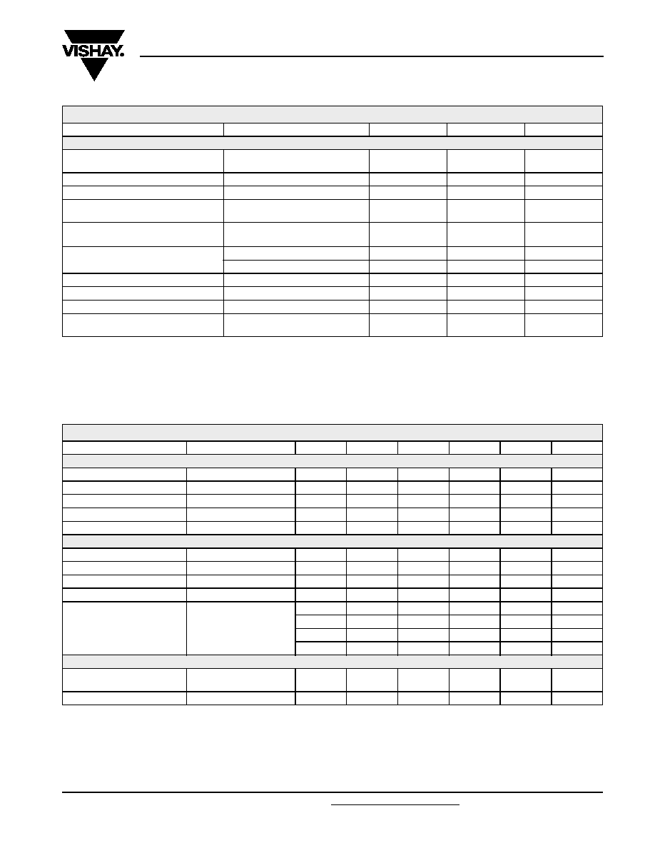
Notes
(1) Tamb = 25 °C, unless otherwise specified.
Stresses in excess of the absolute maximum ratings can cause permanent damage to the device. Functional operation of the device is not
implied at these or any other conditions in excess of those given in the operational sections of this document. Exposure to absolute maximum
ratings for extended periods of the time can adversely affect reliability.
(2) Refer to reflow profile for soldering conditions for surface mounted devices (SMD). Refer to wave profile for soldering conditions for through
hole devices (DIP).
Note
Tamb = 25 °C, unless otherwise specified.
Minimum and maximum values are testing requirements. Typical values are characteristics of the device and are the result of engineering
evaluation. Typical values are for information only and are not part of the testing requirements.
COUPLER
Isolation test voltage
between emitter and detector
t = 1.0 s
VISO
5300
VRMS
Creepage distance
≥ 7mm
Clearance distance
≥ 7mm
Isolation thickness between emitter
and detector
≥ 0.4
mm
Comparative tracking index per
DIN IEC 112/VDE 0303, part 1
175
Isolation resistance
VIO = 500 V, Tamb = 25 °C
RIO
≥ 1012
Ω
VIO = 500 V, Tamb = 100 °C
RIO
≥ 1011
Ω
Storage temperature range
Tstg
- 55 to + 150
°C
Ambient temperature range
Tamb
- 55 to + 100
°C
Junction temperature
max. 10 s, dip soldering
Tj
100
°C
Soldering temperature (2)
max. 10 s, dip soldering:
distance to seating plane
≥ 1.5 mm
Tsld
260
°C
ELECTRICAL CHARACTERISTICS
PARAMETER
TEST CONDITION
PART
SYMBOL
MIN.
TYP.
MAX.
UNIT
INPUT
Forward voltage
IF = 60 mA
VF
1.25
1.65
V
Breakdown voltage
IR = 10 A
VBR
6V
Reverse current
VR = 6 V
IR
0.01
10
A
Capacitance
VF = 0 V, f = 1 MHz
CO
25
pF
Thermal resistance
Rthja
750
K/W
OUTPUT
Collector emitter capacitance
f = 1 MHz, VCE = 5 V
CCE
5.2
pF
Collector base capacitance
f = 1 MHz, VCB = 5 V
CCB
6.5
pF
Emitter base capacitance
f = 1 MHz, VEB = 5 V
CEB
9.5
pF
Thermal resistance
Rthja
500
K/W
Collector emitter leakage
current
VCE = 10 V
SFH600-0
ICEO
235
nA
SFH600-1
ICEO
235
nA
SFH600-2
ICEO
235
nA
SFH600-3
ICEO
570
nA
COUPLER
Saturation voltage collector
emitter voltage
IF = 10 mA, IC = 2.5 mA
VCEsat
0.25
0.4
V
Capacitance (input to output)
CIO
0.6
pF
ABSOLUTE MAXIMUM RATINGS (1)
PARAMETER
TEST CONDITION
SYMBOL
VALUE
UNIT
相关PDF资料 |
PDF描述 |
|---|---|
| SFH601-3X017 | 1 CHANNEL TRANSISTOR OUTPUT OPTOCOUPLER |
| SE3470-001 | INFRARED LED |
| SFH610A-2-X003T | 1 CHANNEL TRANSISTOR OUTPUT OPTOCOUPLER |
| SFH615A-3-X003T | 1 CHANNEL TRANSISTOR OUTPUT OPTOCOUPLER |
| SFH618A-3-X001T | 1 CHANNEL TRANSISTOR OUTPUT OPTOCOUPLER |
相关代理商/技术参数 |
参数描述 |
|---|---|
| SFH600-3X007 | 功能描述:晶体管输出光电耦合器 Phototransistor Out Single CTR>160-320% RoHS:否 制造商:Vishay Semiconductors 输入类型:DC 最大集电极/发射极电压:70 V 最大集电极/发射极饱和电压:0.4 V 绝缘电压:5300 Vrms 电流传递比:100 % to 200 % 最大正向二极管电压:1.65 V 最大输入二极管电流:60 mA 最大集电极电流:100 mA 最大功率耗散:100 mW 最大工作温度:+ 110 C 最小工作温度:- 55 C 封装 / 箱体:DIP-4 封装:Bulk |
| SFH600-4 | 制造商:未知厂家 制造商全称:未知厂家 功能描述:OPTICALLY COUPLED ISOLATOR PHOTOTRANSISTOR OUTPUT |
| SFH601 | 制造商:VISHAY 制造商全称:Vishay Siliconix 功能描述:Optocoupler, Phototransistor Output, With Base Connection |
| SFH601_08 | 制造商:VISHAY 制造商全称:Vishay Siliconix 功能描述:Optocoupler, Phototransistor Output, with Base Connection |
| SFH6011 | 制造商:SIE 功能描述:SFH601-1 SIEMANS S4A1B |
发布紧急采购,3分钟左右您将得到回复。