- 您现在的位置:买卖IC网 > PDF目录85347 > SFH601-4 (VISHAY INTERTECHNOLOGY INC) 1 CHANNEL TRANSISTOR OUTPUT OPTOCOUPLER PDF资料下载
参数资料
| 型号: | SFH601-4 |
| 厂商: | VISHAY INTERTECHNOLOGY INC |
| 元件分类: | 光电耦合器 |
| 英文描述: | 1 CHANNEL TRANSISTOR OUTPUT OPTOCOUPLER |
| 文件页数: | 1/4页 |
| 文件大小: | 499K |
| 代理商: | SFH601-4 |
Document Number: 83663
www.vishay.com
Revision 17-August-01
2–221
SFH601
TRIOS Phototransistor Optocoupler
FEATURES
High Current Transfer Ratios
SFH601-1, 40 to 80%
SFH601-2, 63 to 125%
SFH601-3,100 to 200%
SFH601-4, 160 to 320%
Isolation Test Voltage (1.0 s), 5300 VRMS
VCEsat 0.25 (≤0.4) V, IF=10 mA, IC=2.5 mA
Built to conform to VDE Requirements
Highest Quality Premium Device
Long Term Stability
Storage Temperature, –55
° to +150°C
Field Effect Stable by TRIOS (TRansparent
IOn Shield)
Underwriters Lab File #E52744
CECC Approved
VDE 0884 Available with Option 1
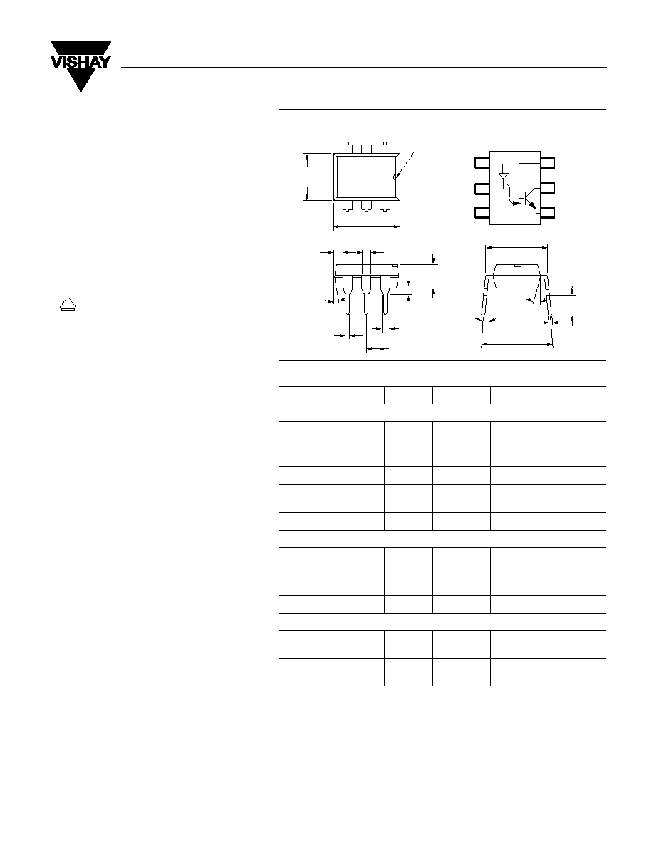
DESCRIPTION
The SFH601 is an optocoupler with a Gallium Ars-
enide LED emitter which is optically coupled with
a silicon planar phototransistor detector. The
component is packaged in a plastic plug-in case
20 AB DIN 41866.
The coupler transmits signals between two elec-
trically isolated circuits.
Maximum Ratings
Emitter
Reverse Voltage ............................................6.0 V
DC Forward Current ....................................60 mA
Surge Forward Current (tp=10 s) ................2.5 A
Total Power Dissipation ............................100 mW
Detector
Collector-Emitter Voltage............................. 100 V
Emitter-Base Voltage .....................................7.0 V
Collector Current .........................................50 mA
Collector Current (t=1.0 ms) .....................100 mA
Power Dissipation.....................................150 mW
Package
Isolation Test Voltage (between emitter and
detector referred to climate DIN 40046,
part 2, Nov. 74) (t=1.0 s) .................. 5300 VRMS
Creepage ...............................................
≥7.0 mm
Clearance...............................................
≥7.0 mm
Isolation Thickness between Emitter and
Detector ..............................................
≥0.4 mm
Comparative Tracking Index per
DIN IEC 112/VDE0303, part 1 ..................... 175
Isolation Resistance
VIO=500 V, TA=25°C ............................ ≥10
12
VIO=500 V, TA=100°C .......................... ≥10
11
Storage Temperature Range ......–55
°C to +150°C
Ambient Temperature Range .....–55
°C to +100°C
Junction Temperature.................................. 100
°C
Soldering Temperature (max. 10 s, dip
soldering: distance to seating plane
≥1.5 mm)..................................................260°C
V
DE
Characteristics (TA=25°C)
Symbol
Unit
Condition
Emitter
Forward Voltage
VF
1.25
(
≤1.65)
V
IF=60 mA
Breakdown Voltage
VBR
≥6.0
V
IR=10 A
Reverse Current
IR
0.01 (
≤10)
A
VR=6.0 V
Capacitance
CO
25
pF
VF=0 V
f=1.0 MHz
Thermal Resistance
RTHJamb
750
K/W
Detector
Capacitance
Collector-Emitter
Collector-Base
Emitter-Base
CCE
CCB
CEB
6.8
8.5
11
pF
f=1.0 MHz
VCE=5.0 V
VCB=5.0 V
VEB=5.0 V
Thermal Resistance
RTHJamb
500
K/W
Package
Saturation Voltage,
Collector-Emitter
VCEsat
0.25 (
≤0.4)
V
IF=10 mA,
IC=2.5 mA
Coupling Capacitance
CIO
0.6
pF
VI-O=0
f=1.0 MHz
.010 (.25)
typ.
.114 (2.90)
.130 (3.0)
.130 (3.30)
.150 (3.81)
.031 (0.80) min.
.300 (7.62)
typ.
.031 (0.80)
.035 (0.90)
.100 (2.54) typ.
.039
(1.00)
Min.
.018 (0.45)
.022 (0.55)
.048 (0.45)
.022 (0.55)
.248 (6.30)
.256 (6.50)
.335 (8.50)
.343 (8.70)
pin one ID
6
5
4
1
2
3
18
°
3
°–9°
.300–.347
(7.62–8.81)
4
°
typ.
Dimensions in inches (mm)
1
2
3
6
5
4
Base
Collector
Emitter
Anode
Cathode
NC
相关PDF资料 |
PDF描述 |
|---|---|
| SEL4226CTP4 | SINGLE COLOR LED, HIGH INTENSITY RED, 4 mm |
| SEL4925DTP1 | SINGLE COLOR LED, ORANGE, 4 mm |
| SEL4717YTP8 | SINGLE COLOR LED, YELLOW, 2 mm |
| SFH617A-2-X019 | 1 CHANNEL TRANSISTOR OUTPUT OPTOCOUPLER |
| SEL1724YTP3 | SINGLE COLOR LED, YELLOW, 4.9 mm |
相关代理商/技术参数 |
参数描述 |
|---|---|
| SFH601-4-009 | 制造商:Siemens 功能描述:Optocoupler, DC Input, Transistor Output, 1 Channel, 5.3KV Isolation, SO |
| SFH601-4X001 | 功能描述:晶体管输出光电耦合器 Phototransistor Out Single CTR>160-320% RoHS:否 制造商:Vishay Semiconductors 输入类型:DC 最大集电极/发射极电压:70 V 最大集电极/发射极饱和电压:0.4 V 绝缘电压:5300 Vrms 电流传递比:100 % to 200 % 最大正向二极管电压:1.65 V 最大输入二极管电流:60 mA 最大集电极电流:100 mA 最大功率耗散:100 mW 最大工作温度:+ 110 C 最小工作温度:- 55 C 封装 / 箱体:DIP-4 封装:Bulk |
| SFH601-4X006 | 功能描述:晶体管输出光电耦合器 Phototransistor Out Single CTR>160-320% RoHS:否 制造商:Vishay Semiconductors 输入类型:DC 最大集电极/发射极电压:70 V 最大集电极/发射极饱和电压:0.4 V 绝缘电压:5300 Vrms 电流传递比:100 % to 200 % 最大正向二极管电压:1.65 V 最大输入二极管电流:60 mA 最大集电极电流:100 mA 最大功率耗散:100 mW 最大工作温度:+ 110 C 最小工作温度:- 55 C 封装 / 箱体:DIP-4 封装:Bulk |
| SFH601-4X006T | 制造商:Vishay Semiconductors 功能描述:SFH601-4X006T - Tape and Reel |
| SFH601-4X007 | 功能描述:晶体管输出光电耦合器 Phototransistor Out Single CTR>160-320% RoHS:否 制造商:Vishay Semiconductors 输入类型:DC 最大集电极/发射极电压:70 V 最大集电极/发射极饱和电压:0.4 V 绝缘电压:5300 Vrms 电流传递比:100 % to 200 % 最大正向二极管电压:1.65 V 最大输入二极管电流:60 mA 最大集电极电流:100 mA 最大功率耗散:100 mW 最大工作温度:+ 110 C 最小工作温度:- 55 C 封装 / 箱体:DIP-4 封装:Bulk |
发布紧急采购,3分钟左右您将得到回复。