- 您现在的位置:买卖IC网 > PDF目录26869 > SFH608-2 (VISHAY INTERTECHNOLOGY INC) 1 CHANNEL TRANSISTOR OUTPUT OPTOCOUPLER PDF资料下载
参数资料
| 型号: | SFH608-2 |
| 厂商: | VISHAY INTERTECHNOLOGY INC |
| 元件分类: | 光电耦合器 |
| 英文描述: | 1 CHANNEL TRANSISTOR OUTPUT OPTOCOUPLER |
| 封装: | PLASTIC, DIP-6 |
| 文件页数: | 1/3页 |
| 文件大小: | 470K |
| 代理商: | SFH608-2 |
Document Number: 83664
www.vishay.com
Revision 17-August-01
2–225
FEATURES
Very High CTR at IF=1.0 mA, VCE=0.5 V
– SFH608-2, 63-125%
– SFH608-3, 100-200%
– SFH608-4, 160-320%
– SFH608-5, 250-500%
Specied Minimum CTR at IF=0.5 mA,
VCE=1.5 V: ≥ 32% (typ. 120%)
Good CTR Linearity with Forward Current
Low CTR Degradation
High Collector-Emitter Voltage VCEO=55 V
Isolation Test Voltage: 5300 VRMS
Low Current Input
Low Coupling Capacitance
High Common Mode Transient Immunity
Phototransistor Optocoupler in 6 Pin DIP
Package
Field Effect Stable by TRIOS (TRansparent IOn
Shield)
VDE 0884 Available with Option 1
Underwriters Lab File #E52744
APPLICATIONS
Telecommunications
Industrial Controls
Ofce Machines
Microprocessor System Interfaces
DESCRIPTION
The SFH 608 is an optocoupler designed for high
current transfer ratio at low input currents with the
output transistor saturated. This makes the device
ideal for low current switching applications. The
SFH608 is packaged in a six pin plastic DIP.
V
DE
Maximum Ratings (TA=25°C)
Emitter
Reverse Voltage ................................................................................... 6.0 V
DC Forward Current ........................................................................... 50 mA
Surge Forward Current (tp
≤10 s) .......................................................2.5 A
Total Power Dissipation .................................................................... 70 mW
Detector
Collector-Emitter Voltage ...................................................................... 55 V
Collector-Base Voltage.......................................................................... 55 V
Emitter-Base Voltage ........................................................................... 7.0 V
Collector Current ............................................................................... 50 mA
Surge Collector Current (tp
≤1.0 ms) ................................................100 mA
Total Power Dissipation .................................................................. 150 mW
Isolation Test Voltage (between emitter and detector, refer
to climate DIN 40046 part 2 Nov. 74) (t=1.0 s)........................ 5300 VRMS
Creepage ......................................................................................
≥7.0 mm
Clearance......................................................................................
≥7.0 mm
Comparative Tracking Index
per DIN IEC 112/VDE 0303, part1 ...................................................... 175
Isolation Resistance
VIO=500 V, TA=25°C .................................................................... ≥10
12
VIO=500 V, TA=100°C ................................................................. ≥10
11
Storage Temperature Range ............................................. –55
°C to +150°C
Operating Temperature Range ......................................... –55
°C to +100°C
Junction Temperature......................................................................... 100
°C
Soldering Temperature (max. 10 s, dip soldering:
distance to seating plane
≥1.5 mm)................................................ 260°C
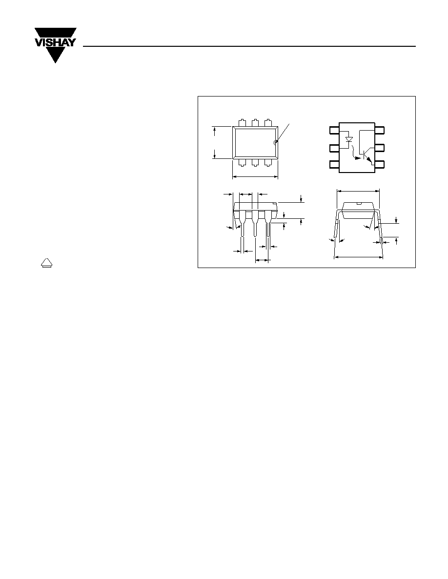
.010 (.25)
typ.
.114 (2.90)
.130 (3.0)
.130 (3.30)
.150 (3.81)
.031 (0.80) min.
.300 (7.62)
typ.
.031 (0.80)
.035 (0.90)
.100 (2.54) typ.
.039
(1.00)
Min.
.018 (0.45)
.022 (0.55)
.048 (0.45)
.022 (0.55)
.248 (6.30)
.256 (6.50)
.335 (8.50)
.343 (8.70)
pin one ID
6
5
4
1
2
3
18
°
3
°–9°
.300–.347
(7.62–8.81)
4
°
typ.
Dimensions in inches (mm)
1
2
3
6
5
4
Base
Collector
Emitter
Anode
Cathode
NC
SFH608
5.3 KV, TRIOS, Low Current
Phototransistor Optocoupler
相关PDF资料 |
PDF描述 |
|---|---|
| SFH608-3-X006 | 1 CHANNEL TRANSISTOR OUTPUT OPTOCOUPLER |
| SFH608-3-X009 | 1 CHANNEL TRANSISTOR OUTPUT OPTOCOUPLER |
| SFH608-4-X006 | 1 CHANNEL TRANSISTOR OUTPUT OPTOCOUPLER |
| SFH608-2-X009T | 1 CHANNEL TRANSISTOR OUTPUT OPTOCOUPLER |
| SFH608-4-X017 | 1 CHANNEL TRANSISTOR OUTPUT OPTOCOUPLER |
相关代理商/技术参数 |
参数描述 |
|---|---|
| SFH608-2X006 | 制造商:Vishay Angstrohm 功能描述:Optocoupler DC-IN 1-CH Transistor With Base DC-OUT 制造商:Vishay Semiconductors 功能描述:DIP-6 CPL 63-125% CTR -E3 - Tape and Reel 制造商:Vishay Semiconductors 功能描述:DIP-6 CPL 63-125% CTR 制造商:Vishay Semiconductors 功能描述:OPTOCOUPLER, PHOTOTRANSISTOR O/P, 5.3KV, DIP-6; No. of Channels:1; Isolation Voltage:5.3kV; Optocoupler Output Type:Phototransistor; Input Current:50mA; Output Voltage:55V; Opto Case Style:DIP; No. of Pins:6 ;RoHS Compliant: Yes |
| SFH608-2-X006 | 制造商:VISHAY 制造商全称:Vishay Siliconix 功能描述:Optocoupler, Phototransistor Output, Low Input Current, With Base Connection, 5300 VRMS |
| SFH608-2-X007 | 制造商:VISHAY 制造商全称:Vishay Siliconix 功能描述:Optocoupler, Phototransistor Output, Low Input Current, With Base Connection, 5300 VRMS |
| SFH608-2-X009 | 制造商:VISHAY 制造商全称:Vishay Siliconix 功能描述:Optocoupler, Phototransistor Output, Low Input Current, With Base Connection, 5300 VRMS |
| SFH608-3 | 功能描述:晶体管输出光电耦合器 Phototransistor Out Single CTR 100-200% RoHS:否 制造商:Vishay Semiconductors 输入类型:DC 最大集电极/发射极电压:70 V 最大集电极/发射极饱和电压:0.4 V 绝缘电压:5300 Vrms 电流传递比:100 % to 200 % 最大正向二极管电压:1.65 V 最大输入二极管电流:60 mA 最大集电极电流:100 mA 最大功率耗散:100 mW 最大工作温度:+ 110 C 最小工作温度:- 55 C 封装 / 箱体:DIP-4 封装:Bulk |
发布紧急采购,3分钟左右您将得到回复。