- 您现在的位置:买卖IC网 > PDF目录85216 > SFH615A-12-X001 (VISHAY INTERTECHNOLOGY INC) 1 CHANNEL TRANSISTOR OUTPUT OPTOCOUPLER PDF资料下载
参数资料
| 型号: | SFH615A-12-X001 |
| 厂商: | VISHAY INTERTECHNOLOGY INC |
| 元件分类: | 光电耦合器 |
| 英文描述: | 1 CHANNEL TRANSISTOR OUTPUT OPTOCOUPLER |
| 封装: | PLASTIC, DIP-4 |
| 文件页数: | 1/4页 |
| 文件大小: | 262K |
| 代理商: | SFH615A-12-X001 |
2000 Inneon Technologies Corp. Optoelectronics Division San Jose, CA
www.inneon.com/opto 1-888-Inneon (1-888-463-4636)
OSRAM Opto Semiconductors GmbH & Co. OHG Regensburg, Germany
www.osram-os.com +49-941-202-7178
1
February 23, 2000-14
SFH615A
5.3 kV
TRIOS Optocoupler
High Reliability
FEATURES
Variety of Current Transfer Ratios at IF=10 mA
– SFH615A-1, 40–80%
– SFH615A-2, 63–125%
– SFH615A-3, 100–200%
– SFH615A-4, 160–320%
– SFH615A-12, 40–125%
– SFH615A-23, 63–200%
– SFH615A-34, 100–320%
– SFH615A-13, 40–200%
– SFH615A-24, 63–320%
– SFH615A-14, 40–320%
Low CTR Degradation
Good CTR Linearity Depending on Forward
Current
Withstand Test Voltage, 5300 VRMS
High Collector-Emitter Voltage, VCEO=70 V
Low Saturation Voltage
Fast Switching Times
Field-Effect Stable by TRIOS
(TRansparent IOn Shield)
Temperature Stable
Low Coupling Capacitance
End-Stackable, .100" (2.54 mm) Spacing
High Common-Mode Interference Immunity
(Unconnected Base)
Underwriters Lab File #52744
VDE 0884 Available with Option 1
DESCRIPTION
The SFH615A features a large variety of transfer ratio,
low coupling capacitance and high isolation voltage.
These couplers have a GaAs infrared emitting diode
emitter, which is optically coupled to a silicon planar
phototransistor detector, and is incorporated in a plas-
tic DIP-4 package.
The coupling devices are designed for signal transmis-
sion between two electrically separated circuits.
The couplers are end-stackable with 2.54 mm lead
spacing.
Creepage and clearance distances of >8.0 mm are
achieved with option 6. This version complies with IEC
950 (DIN VDE 0805) for reinforced insulation up to an
operation voltage of 400 VRMS or DC.
Specications subject to change.
V
DE
Maximum Ratings
Emitter
Reverse Voltage ...............................................................................6.0 V
DC Forward Current ...................................................................... 60 mA
Surge Forward Current (tP≤10 s) ....................................................2.5 A
Total Power Dissipation .............................................................. 100 mW
Detector
Collector-Emitter Voltage...................................................................70 V
Emitter-Collector Voltage..................................................................7.0 V
Collector Current ........................................................................... 50 mA
Collector Current (tP≤1.0 ms) ...................................................... 100 mA
Total Power Dissipation .............................................................. 150 mW
Package
Isolation Test Voltage between Emitter and
Detector, refer to Climate DIN 40046,
part 2, Nov. 74, t=1.0 s ....................................................... 5300 VRMS
Creepage ....................................................................................
≥7.0 mm
Clearance....................................................................................
≥7.0 mm
Insulation Thickness between Emitter and Detector .................
≥0.4 mm
Comparative Tracking Index
per DIN IEC 112/VDE0 303, part 1................................................
≥175
Isolation Resistance
VIO=500 V, TA=25°C ................................................................ ≥10
12
VIO=500 V, TA=100°C .............................................................. ≥10
11
Storage Temperature Range..............................................–55 to +150
°C
Ambient Temperature Range ............................................–55 to +100
°C
Junction Temperature..................................................................... 100
°C
Soldering Temperature (max. 10 s. Dip Soldering
Distance to Seating Plane
≥1.5 mm) .......................................... 260°C
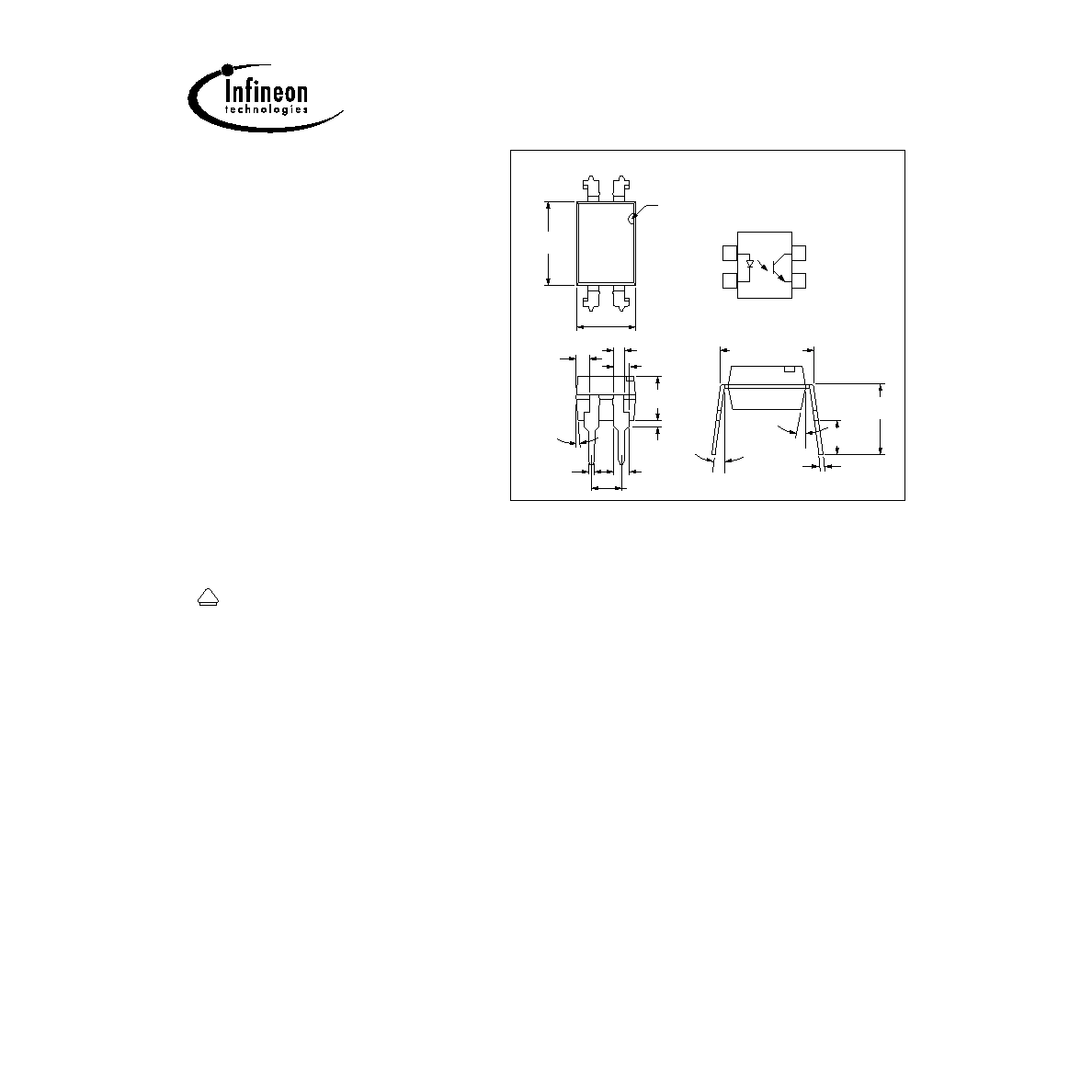
.255 (6.48)
.268 (6.81)
1
2
4
3
.179 (4.55)
.190 (4.83)
pin one ID
.030 (.76)
.045 (1.14)
4
°
typ.
0.100 (2.54)
.130 (3.30)
.150 (3.81)
.020 (.508 )
.035 (.89)
10
°
3
°–9°
.018 (.46)
.022 (.56)
.008 (.20)
.012 (.30)
.031 (.79) typ.
.050 (1.27) typ.
.300 (7.62) typ.
.110 (2.79)
.130 (3.30)
.230 (5.84)
.250 (6.35)
.050 (1.27)
Dimensions in inches (mm)
1
2
4
3
Anode
Collector
Cathode
Emitter
相关PDF资料 |
PDF描述 |
|---|---|
| SFH615A-24-X001 | 1 CHANNEL TRANSISTOR OUTPUT OPTOCOUPLER |
| SEL4117RTP8 | SINGLE COLOR LED, RED, 2 mm |
| SEL2111RTP7 | SINGLE COLOR LED, RED, 3.1 mm |
| SFH601-3 | 1 CHANNEL TRANSISTOR OUTPUT OPTOCOUPLER |
| SEL1724YTP2 | SINGLE COLOR LED, YELLOW, 4.9 mm |
相关代理商/技术参数 |
参数描述 |
|---|---|
| SFH615A-1X001 | 功能描述:晶体管输出光电耦合器 Phototransistor Out Single CTR > 40-80% RoHS:否 制造商:Vishay Semiconductors 输入类型:DC 最大集电极/发射极电压:70 V 最大集电极/发射极饱和电压:0.4 V 绝缘电压:5300 Vrms 电流传递比:100 % to 200 % 最大正向二极管电压:1.65 V 最大输入二极管电流:60 mA 最大集电极电流:100 mA 最大功率耗散:100 mW 最大工作温度:+ 110 C 最小工作温度:- 55 C 封装 / 箱体:DIP-4 封装:Bulk |
| SFH615A-1X006 | 功能描述:晶体管输出光电耦合器 Phototransistor Out Single CTR > 40-80% RoHS:否 制造商:Vishay Semiconductors 输入类型:DC 最大集电极/发射极电压:70 V 最大集电极/发射极饱和电压:0.4 V 绝缘电压:5300 Vrms 电流传递比:100 % to 200 % 最大正向二极管电压:1.65 V 最大输入二极管电流:60 mA 最大集电极电流:100 mA 最大功率耗散:100 mW 最大工作温度:+ 110 C 最小工作温度:- 55 C 封装 / 箱体:DIP-4 封装:Bulk |
| SFH615A-1X007 | 制造商:VISHAY 制造商全称:Vishay Siliconix 功能描述:Optocoupler, Phototransistor Output, High Reliability, 5300 VRMS |
| SFH615A-1X008T | 制造商:Vishay Angstrohm 功能描述:Optocoupler DC-IN 1-CH Transistor DC-OUT T/R 制造商:Vishay Semiconductors 功能描述:SMD-4 CPL 40-80% CTR -E3 - Tape and Reel 制造商:Vishay Semiconductors 功能描述:SMD-4 CPL 40-80% CTR 制造商:Vishay Semiconductors 功能描述:OPTOCOUPLER, PHOTOTRANSISTOR O/P, 5.3KV, SMD-4; No. of Channels:1; Isolation Voltage:5.3kV; Optocoupler Output Type:Phototransistor; Input Current:60mA; Output Voltage:70V; Opto Case Style:SMD; No. of Pins:4 ;RoHS Compliant: Yes |
| SFH615A-1X016 | 功能描述:晶体管输出光电耦合器 Phototransistor Out Single CTR > 40-80% RoHS:否 制造商:Vishay Semiconductors 输入类型:DC 最大集电极/发射极电压:70 V 最大集电极/发射极饱和电压:0.4 V 绝缘电压:5300 Vrms 电流传递比:100 % to 200 % 最大正向二极管电压:1.65 V 最大输入二极管电流:60 mA 最大集电极电流:100 mA 最大功率耗散:100 mW 最大工作温度:+ 110 C 最小工作温度:- 55 C 封装 / 箱体:DIP-4 封装:Bulk |
发布紧急采购,3分钟左右您将得到回复。