- 您现在的位置:买卖IC网 > PDF目录66215 > SFH6318T (VISHAY INTERTECHNOLOGY INC) 1 CHANNEL LOGIC OUTPUT OPTOCOUPLER PDF资料下载
参数资料
| 型号: | SFH6318T |
| 厂商: | VISHAY INTERTECHNOLOGY INC |
| 元件分类: | 光电耦合器 |
| 英文描述: | 1 CHANNEL LOGIC OUTPUT OPTOCOUPLER |
| 封装: | SOIC-8 |
| 文件页数: | 2/3页 |
| 文件大小: | 385K |
| 代理商: | SFH6318T |
Document Number: 83678
www.vishay.com
Revision 17-August-01
2–283
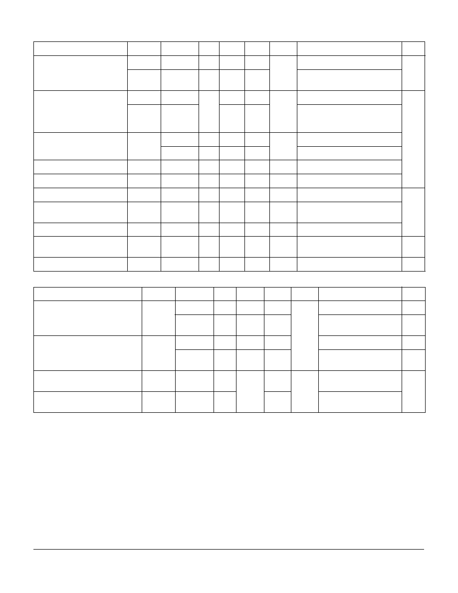
Electro-Optical Characteristics (TA=0°C to 70°C, TA=25°C—Typical, unless otherwise specied)
Switching Specications (TA=25°C)
Notes
1. DC current transfer ratio is dened as the ratio of output collector current, IO, to the forward LED input current, IF times 100%.
2. Pin 7 open.
3. Device considered a two-terminal device: pins 1, 2, 3 and 4 shorted together and pins 5, 6, 7 and 8 shorted together.
4. Using a resistor between pin 5 and 7 will decrease gain and delay time.
5. Common mode transient immunity in logic high level is the maximum tolerable (positive) dVcm/dt on the leading edge of the common mode
pulse, VCM, to assure that the output will remain in a logic high state (i.e. VO>2.0 V) common mode transient immunity in logic low level is the
maximum tolerable (negative) dVcm/dt on the trailing edge of the common mode pulse signal, VCM, to assure that the output will remain in a logic
low state (i.e. VO<0.8 V).
6. In applications where dv/dt may exceed 50,000 V/
s (such as state discharge) a series resistor, RCC should be included to protect IC from
destructively high surge currents. The recommended value is
Refer to Figure 2.
Parameter
Symbol
Device
Min
Typ
Max
Units
Test Conditions
Note
Current Transfer Ratio
CTR
SFH6318T
300
1600
2600
%
IF=1.6 mA, VO=0.4 V, VCC=4.5 V
1,2
—
SFH6319T
400
500
2000
1600
3500
2600
IF=0.5 mA, VO=0.4 V, VCC=4.5 V
IF=1.6 mA, VO=0.4 V, VCC=4.5 V
Logic Low
Output Voltage
VOL
SFH6318T
—
0.1
0.4
V
IF=1.6 mA, IO=4.8 mA, VCC=4.5 V
2
—
SFH6319T
0.1
0.15
0.25
0.4
IF=1.6 mA, IO=8.0 mA, VCC=4.5 V
IF=5.0 mA, IO=15 mA, VCC=4.5 V
IF=12 mA, IO=24 mA, VCC=4.5 V
Logic High
Output Current
IOH
SFH6318T
—
0.1
250
A
IF=0 mA, VO=VCC=7.0 V
SFH6319T
—
0.05
100
IF=0 mA, VO=VCC=18 V
Logic Low Supply Current
ICCL
—
0.2
1.5
mA
IF=1.6 mA, VO=OPEN, VCC=18 V
Logic High Supply Current
ICCH
—
0.01
10
A
IF=0 mA, VO=OPEN, VCC=18 V
Input Forward Voltage
VF
—
1.4
1.7
V
IF=1.6 mA, TA=25°C—
Temperature Coefficient,
Forward Voltage
VF/TA
—
–1.8
—
mV/
°C
IF=1.6 mA
Input Capacitance
CIN
—
25
—
pF
f=1.0 MHz, VF=0
Resistance (Input-Output)
RI-O
——
1012
1011
—
VIO=500 VDC, TA=25°C
VIO=500 VDC, TA=100°C
3
Capacitance (Input-Output)
CI-O
—
0.6
—
pF
f=1.0 MHz
3
Parameter
Symbol
Device
Min
Typ
Max
Units
Test Conditions
Note
Propagation Delay Time
To Logic Low at Output
tPHL
SFH6318T
—
2.0
10
s
IF=1.6 mA, RL=2.2 k
SFH6319T
—
6.0
0.6
25
1.0
IF=0.5 mA, RL=4.7 k
IF=12 mA, RL=270
2,4
Propagation Delay Time
To Logic High at Output
tPLH
SFH6318T
—
2.0
35
IF=1.6 mA, RL=2.2 k
—
SFH6319T
—
4.0
1.5
60
7.0
IF=0.5 mA, RL=4.7 k
IF=12 mA, RL=270
2,4
Common Mode Transient Immunity
at Logic High Level Output
| CMH |
—
1 K
—
V/
s
IF=0 mA, RL=2.2 k
VCM=10 VP–P
5,6
Common Mode Transient Immunity
at Logic Low Level Output
| CML|—
—
IF=1.6 mA, RL=2.2 k
VCM=10 VP–P
R
CC
IV
0.15 I
F
mA
()
-------------------------------k
相关PDF资料 |
PDF描述 |
|---|---|
| SFH6326 | 2 CHANNEL LOGIC OUTPUT OPTOCOUPLER, 1 Mbps |
| SFH6326 | 2 CHANNEL LOGIC OUTPUT OPTOCOUPLER, 1 Mbps |
| SFH6326 | 1 CHANNEL LOGIC OUTPUT OPTOCOUPLER, 1 Mbps |
| SFH6345-X001 | 1 CHANNEL LOGIC OUTPUT OPTOCOUPLER, 1 Mbps |
| SFH6345-X017 | 1 CHANNEL LOGIC OUTPUT OPTOCOUPLER, 1 Mbps |
相关代理商/技术参数 |
参数描述 |
|---|---|
| SFH6318T | 制造商:Vishay Semiconductors 功能描述:Optocoupler |
| SFH6319 | 制造商:INFINEON 制造商全称:Infineon Technologies AG 功能描述:LOW CURRENT, HIGH GAIN OPTOCOUPLER |
| SFH6319 | 制造商:Vishay Intertechnologies 功能描述:OPTOCOUPLER SMD TRANSISTOR O/P |
| SFH6319T | 功能描述:高速光耦合器 100kbd Low Input Current High Gain RoHS:否 制造商:Avago Technologies 电流传递比: 最大波特率: 最大正向二极管电压:1.75 V 最大反向二极管电压:5 V 最大功率耗散:40 mW 最大工作温度:+125 C 最小工作温度:- 40 C 封装 / 箱体:SOIC-5 封装:Tube |
| SFH6319-T | 制造商:Vishay Angstrohm 功能描述:Optocoupler DC-IN 1-CH Darlington With Base DC-OUT 8-Pin SOIC N T/R 制造商:Vishay 功能描述:Optocoupler DC-IN 1-CH Darlington With Base DC-OUT 8-Pin SOIC N T/R |
发布紧急采购,3分钟左右您将得到回复。