- 您现在的位置:买卖IC网 > PDF目录85347 > SFH6325 (VISHAY INTERTECHNOLOGY INC) 1 CHANNEL LOGIC OUTPUT OPTOCOUPLER, 1 Mbps PDF资料下载
参数资料
| 型号: | SFH6325 |
| 厂商: | VISHAY INTERTECHNOLOGY INC |
| 元件分类: | 光电耦合器 |
| 英文描述: | 1 CHANNEL LOGIC OUTPUT OPTOCOUPLER, 1 Mbps |
| 封装: | PLASTIC, DIP-8 |
| 文件页数: | 1/5页 |
| 文件大小: | 451K |
| 代理商: | SFH6325 |
Document Number: 83679
www.vishay.com
Revision 17-August-01
2–285
SFH6325/SFH6326
High-Speed Dual Optocoupler
FEATURES
Isolation Test Voltage: 5300 VRMS
TTL Compatible
Bit Rates: 1.0 MBit/s
High Common-mode Transient Immunity
Bandwidth 2.0 MHz
Open-Collector Output
Field-effect Stable by TRIOS
(TRansparent IOn Shield)
Underwriters Lab File #E52744
Description
The SFH6325/6326 are dual channel optocouplers
with a GaAIAs infrared emitting diode, optically
coupled with an integrated photodetector which
consists of a photodiode and a high-speed transis-
tor in a DIP-8 plastic package.
Signals can be transmitted between two electrically
separated circuits up to frequencies of 2.0 MHz.
The potential difference between the circuits to be
coupled is not allowed to exceed the maximum per-
missible reference voltages.
Maximum Ratings, TA=25°C
Emitter (each channel)
Reverse Voltage ...................................................................................4.5 V
Continuous Forward Current ..............................................................25 mA
Peak Forward Current
(t=1.0 ms, duty cycle 50%) .............................................................50 mA
Maximum Surge Forward Current
(t
≤1.0 s, 300 pulses/s).....................................................................1.0 A
Derate Linearly from 25
°C.......................................................... 0.6 mW/°C
Total Power Dissipation (TA≤70°C) ....................................................50 mW
Detector (each channel)
Supply Voltage .......................................................................... –0.5 to 30 V
Output Voltage .......................................................................... –0.5 to 25 V
Collector Output Current ...................................................................8.0 mA
Derate Linearly from 25
°C........................................................ 1.33 mW/°C
Total Power Dissipation (TA≤70°C) ....................................................50 mW
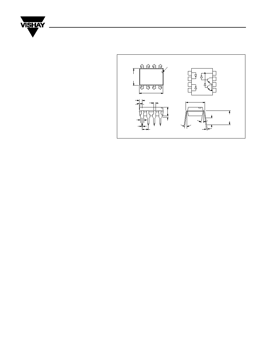
Package
Isolation Test Voltage (t=1.0 s) ...................................................5300 VRMS
Pollution Degree (DIN VDE 0109) .............................................................. 2
Creepage ......................................................................................
≥7.0 mm
Clearance ......................................................................................
≥7.0 mm
Derate Linearly from 25
°C........................................................ 1.93 mW/°C
Total Package Dissipation at 25
°C TA .............................................145 mW
Comparative Tracking Index per
DIN IEC112/VDE 0303 part 1,
Group IIIa per DIN VDE 6110 ............................................................... 175
Isolation Resistance
VIO=500 V, TA=25°C ..................................................................... ≥10
12
VIO=500 V, TA=100°C ................................................................... ≥10
11
Storage Temperature Range ............................................ –55
°C to +125°C
Ambient Temperature Range ........................................... –55
°C to +100°C
Soldering Temperature
(max. 10 s, DIP soldering:
distance to seating plane
≥1.5 mm).................................................260°C
pin one ID
.255 (6.48)
.268 (6.81)
.379 (9.63)
.390 (9.91)
.030 (0.76)
.045 (1.14)
4
° typ.
.100 (2.54) typ.
10
°
3
°–9°
.300 (7.62)
typ.
.018 (.46)
.022 (.56)
.008 (.20)
.012 (.30)
.110 (2.79)
.130 (3.30)
.150 (3.81)
.020 (.51)
.035 (.89)
.230 (5.84)
.250 (6.35)
4
3
2
1
.031 (0.79)
.050 (1.27)
5
6
78
1
2
3
4
8
7
6
5
Cathode
(VCC)
Collector1
(V01)
Collector2
(V02)
Emitter
(GND)
Anode1
Cathode1
Cathode2
Anode2
Dimensions in inches (mm)
相关PDF资料 |
PDF描述 |
|---|---|
| S109-0UR-014N | SINGLE COLOR DISPLAY CLUSTER, ULTRA RED |
| SFH601-5G | 1 CHANNEL TRANSISTOR OUTPUT OPTOCOUPLER |
| SL640CY5-36V/80-BP | SINGLE COLOR DISPLAY CLUSTER, AMBER YELLOW, 48.77 mm |
| S330CY5-5V/30-N | SINGLE COLOR LED, AMBER YELLOW, 10.6 mm |
| S606CPG5-6V/90-N | SINGLE COLOR DISPLAY CLUSTER, PURE GREEN, 15.75 mm |
相关代理商/技术参数 |
参数描述 |
|---|---|
| SFH6325_08 | 制造商:VISHAY 制造商全称:Vishay Siliconix 功能描述:High Speed Optocoupler, Dual Channel, 1 MBd, Transistor Output |
| SFH6325-X009 | 功能描述:高速光耦合器 1Mbd High-Speed Tran Out Dual CTR>7% RoHS:否 制造商:Avago Technologies 电流传递比: 最大波特率: 最大正向二极管电压:1.75 V 最大反向二极管电压:5 V 最大功率耗散:40 mW 最大工作温度:+125 C 最小工作温度:- 40 C 封装 / 箱体:SOIC-5 封装:Tube |
| SFH6325-X009T | 制造商:Vishay Angstrohm 功能描述:HIGH SPEED OPTOCOUPLER, DUAL CHANNEL, 1 MBD, TRANSISTOR OUTPUT 制造商:Vishay Semiconductors 功能描述:SMD-8 CPLR DUAL 1MBD CTR>7% -E3 - Tape and Reel 制造商:Vishay Semiconductors 功能描述:OPTOCOUPLER, TRANSISTOR O/P, 5.3KV, SMD-8; No. of Channels:2; Isolation Voltage:5.3kV; Optocoupler Output Type:Transistor; Input Current:25mA; Output Voltage:25V; Opto Case Style:SMD; No. of Pins:8 ;RoHS Compliant: Yes |
| SFH6325-X017T | 功能描述:高速光耦合器 1Mbd High-Speed Tran Out Dual CTR>7% RoHS:否 制造商:Avago Technologies 电流传递比: 最大波特率: 最大正向二极管电压:1.75 V 最大反向二极管电压:5 V 最大功率耗散:40 mW 最大工作温度:+125 C 最小工作温度:- 40 C 封装 / 箱体:SOIC-5 封装:Tube |
| SFH6326 | 功能描述:高速光耦合器 1Mbd Open Collector Dual Channel RoHS:否 制造商:Avago Technologies 电流传递比: 最大波特率: 最大正向二极管电压:1.75 V 最大反向二极管电压:5 V 最大功率耗散:40 mW 最大工作温度:+125 C 最小工作温度:- 40 C 封装 / 箱体:SOIC-5 封装:Tube |
发布紧急采购,3分钟左右您将得到回复。