- 您现在的位置:买卖IC网 > PDF目录85292 > SFH690ABT (VISHAY INTERTECHNOLOGY INC) 1 CHANNEL TRANSISTOR OUTPUT OPTOCOUPLER PDF资料下载
参数资料
| 型号: | SFH690ABT |
| 厂商: | VISHAY INTERTECHNOLOGY INC |
| 元件分类: | 光电耦合器 |
| 英文描述: | 1 CHANNEL TRANSISTOR OUTPUT OPTOCOUPLER |
| 封装: | SOP-4 |
| 文件页数: | 1/4页 |
| 文件大小: | 397K |
| 代理商: | SFH690ABT |
Document Number: 83686
www.vishay.com
Revision 17-August-01
1
FFEATURES
Current Transfer Ratios
– SFH690AT, 50%–150%
– SFH690BT, 100%–300%
– SFH690ABT, 50%–300%
SOP (Small Outline Package)
Isolation Test Voltage, 3750 VRMS (1.0 s)
High Collector-Emitter Breakdown Voltage,
VCEO=70 V
Low Saturation Voltage
Fast Switching Times
Field-Effect Stable by TRIOS
(TRansparent IOn Shield)
Temperature Stable
Low Coupling Capacitance
End-Stackable, .100" (2.54 mm) Spacing
Underwriters Lab File #52744
APPLICATIONS
High density mounting or space sensitive PCBs
PLCs
Telecommunication
DESCRIPTION
The SFH690xT family has a GaAs infrared emitting diode
emitter, which is optically coupled to a silicon planar pho-
totransistor detector, and is incorporated in a 4 pin 100
mil lead pitch miniat package. It features a high current
transfer ratio, low coupling capacitance, and high isola-
tion voltage.
The coupling devices are designed for signal transmis-
sion between two electrically separated circuits.
The SFH690xT will be offered in tape and reel format
only. There are 2000 parts per reel. For the SFH690AT,
the product will be marked as SFH690A and the
SFH690BT will be marked as SFH690B. The
SFH690ABT will be marked as SFH690A or SFH690B.
Absolute Maximum Ratings, TA=25°C (except where noted)
Emitter
Reverse Voltage ............................................................................... 6.0 V
DC Forward Current.......................................................................50 mA
Surge Forward Current (tP≤10 s)....................................................2.5 A
Total Power Dissipation ............................................................... 80 mW
Detector
Collector-Emitter Voltage .................................................................. 70 V
Emitter-Collector Voltage ................................................................. 7.0 V
Collector Current............................................................................50 mA
Collector Current (tP≤1.0 ms).......................................................100 mA
Total Power Dissipation ............................................................. 150 mW
Package
Isolation Test Voltage between Emitter and
Detector (1.0 s)....................................................................3750 VRMS
Creepage
.......................................................................................... ≥5.33 mm
Clearance
.......................................................................................... ≥5.08 mm
Insulation Thickness between Emitter and Detector
.................. ≥0.4 mm
Comparative Tracking Index
per DIN IEC 112/VDE0 303, part 1
.................................................... ≥175
Isolation Resistance
VIO=500 V, TA=25°C........................................................................≥10
12
VIO=500 V, TA=100°C .....................................................................≥10
11
Storage Temperature Range ............................................. –55 to +150
°C
Ambient Temperature Range ............................................ –55 to +100
°C
Junction Temperature .................................................................... 100
°C
Soldering Temperature (max. 10 s Dip Soldering
Distance to Seating Plane
≥1.5 mm).......................................... 260°C
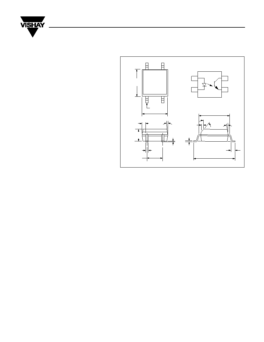
0.190 (4.83)
0.170 (4.32)
0.184 (4.67)
0.164 (4.17)
0.024 (0.61)
0.034 (0.86)
1
4
2
3
0.018 (0.46)
0.014 (0.36)
0.105 (2.67)
0.095 (2.41)
LEADS COPLANARITY
0.004 (0.10)
0.018 (0.46)
0.013 (0.33)
0.025 (0.63)
0.015 (0.38)
0.220 (5.59)
0.200 (5.08)
40
10
0.008 (0.20)
0.004 (0.10)
0.284 (7.21)
0.264 (6.71)
Pin one I.D. (on chamfer side of package)
0.080 (2.03)
0.075 (1.91)
6
Max.
1
2
4
3
Emitter
Collector
Anode
Cathode
Dimensions in inches (mm)
SFH690AT/690BT/690ABT
Phototransistor Optocoupler
Miniat SOP Package
相关PDF资料 |
PDF描述 |
|---|---|
| SLR-342VR | T-1 SINGLE COLOR LED, RED, 3.1 mm |
| SFH6156-3TRIOS | 1 CHANNEL TRANSISTOR OUTPUT OPTOCOUPLER |
| SFH6156-4TRIOS-X001 | 1 CHANNEL TRANSISTOR OUTPUT OPTOCOUPLER |
| S-963-P11 | 3.18 mm SLOT WIDTH, 1 CHANNEL SLOTTED OPTICAL SWITCH LOGIC OUTPUT |
| SPMWHT5206N5C0R0S0 | SINGLE COLOR LED, WHITE, 3.5 mm |
相关代理商/技术参数 |
参数描述 |
|---|---|
| SFH690ABT | 制造商:Vishay Semiconductors 功能描述:Optocoupler |
| SFH690AT | 功能描述:晶体管输出光电耦合器 Phototransistor Out Single CTR 50-150% RoHS:否 制造商:Vishay Semiconductors 输入类型:DC 最大集电极/发射极电压:70 V 最大集电极/发射极饱和电压:0.4 V 绝缘电压:5300 Vrms 电流传递比:100 % to 200 % 最大正向二极管电压:1.65 V 最大输入二极管电流:60 mA 最大集电极电流:100 mA 最大功率耗散:100 mW 最大工作温度:+ 110 C 最小工作温度:- 55 C 封装 / 箱体:DIP-4 封装:Bulk |
| SFH690AT | 制造商:Vishay Semiconductors 功能描述:Optocoupler |
| SFH690AT3 | 功能描述:晶体管输出光电耦合器 SOP-6 CPLR 50-150% CTR -E3 RoHS:否 制造商:Vishay Semiconductors 输入类型:DC 最大集电极/发射极电压:70 V 最大集电极/发射极饱和电压:0.4 V 绝缘电压:5300 Vrms 电流传递比:100 % to 200 % 最大正向二极管电压:1.65 V 最大输入二极管电流:60 mA 最大集电极电流:100 mA 最大功率耗散:100 mW 最大工作温度:+ 110 C 最小工作温度:- 55 C 封装 / 箱体:DIP-4 封装:Bulk |
| SFH690BT | 功能描述:晶体管输出光电耦合器 Phototransistor Out Single CTR 100-300% RoHS:否 制造商:Vishay Semiconductors 输入类型:DC 最大集电极/发射极电压:70 V 最大集电极/发射极饱和电压:0.4 V 绝缘电压:5300 Vrms 电流传递比:100 % to 200 % 最大正向二极管电压:1.65 V 最大输入二极管电流:60 mA 最大集电极电流:100 mA 最大功率耗散:100 mW 最大工作温度:+ 110 C 最小工作温度:- 55 C 封装 / 箱体:DIP-4 封装:Bulk |
发布紧急采购,3分钟左右您将得到回复。