- 您现在的位置:买卖IC网 > PDF目录376349 > SG1842 (Microsemi Corporation) CURRENT MODE PWM CONTROLLER PDF资料下载
参数资料
| 型号: | SG1842 |
| 厂商: | Microsemi Corporation |
| 英文描述: | CURRENT MODE PWM CONTROLLER |
| 中文描述: | 电流模式PWM控制器 |
| 文件页数: | 11/14页 |
| 文件大小: | 224K |
| 代理商: | SG1842 |
C
U R R E N T
-M
O D E
PWM C
O N T R O L L E R
SG1842/SG1843 Series
P R O D U C T D A T A B O O K 1 9 9 6 / 1 9 9 7
11
Copyright 2000
Rev. 1.6 4/00
P
R O D U C T I O N
D
A T A
S
H E E T
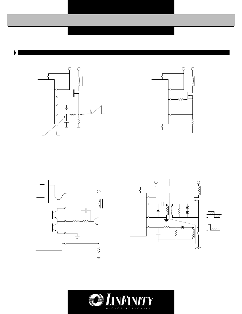
T Y P I C A L A P P L I C AT I O N C I R C U I T S
Pin numbers referenced are for 8-pin package and pin numbers in parenthesis are for 14-pin package.
FIGURE 18.
— ISOLATED MOSFET DRIVE
FIGURE 17.
— BIPOLAR TRANSISTOR DRIVE
Current transformers can be used where isolation is required
between PWM and Primary ground. A drive transformer is then
necessary to interface the PWM output with the MOSFET.
The 1842/43 output stage can provide negative base current to
remove base charge of power transistor (Q
) for faster turn off. This
is accomplished by adding a capacitor (C
) in parallel with a resistor
(R
1
). The resistor (R
1
) is to limit the base current during turn on.
FIGURE 15.
— CURRENT-SENSE SPIKE SUPPRESSION
FIGURE 16.
— MOSFET PARASITIC OSCILLATIONS
A resistor (R
) in series with the MOSFET gate reduce overshoot and
ringing caused by the MOSFET input capacitance and any induc-
tance in series with the gate drive. (Note: It is very important to
have a low inductance ground path to insure correct operation of
the I.C. This can be done by making the ground paths as short and
as wide as possible.)
The RC low pass filter will eliminate the leading edge current spike
caused by parasitics of Power MOSFET.
V
CC
V
IN
7 (12)
7 (11)
6 (10)
5 (8)
3 (5)
R
C
R
S
Q1
I
PK
I
PK(MAX)
=1.0V
R
S
SG1842/43
V
IN
V
CC
7 (12)
7 (11)
6 (10)
5 (8)
R
S
Q1
SG1842/43
3 (5)
R
1
SG1842/43
3 (5)
5 (8)
6 (10)
7 (11)
R
S
Q1
V
C1
C
1
R
1
R
2
V
IN
V
C
I
B
+
V
C
R
2
V
C1
R
1
||R
2
_
V
CC
V
IN
7 (12)
7 (11)
6 (10)
5 (8)
3 (5)
SG1842/43
Isolation
Boundary
C
R
R
S
N
S
N
P
Q1
Waveforms
+
_
+
_
50% DC
25% DC
I
PK
=V (PIN 1) - 1.4
3R
S
N
P
N
S
相关PDF资料 |
PDF描述 |
|---|---|
| SG1842J | CURRENT MODE PWM CONTROLLER |
| SG1842L | CURRENT MODE PWM CONTROLLER |
| SG1842Y | CURRENT MODE PWM CONTROLLER |
| SG1843J | CURRENT MODE PWM CONTROLLER |
| SG1843L | CURRENT MODE PWM CONTROLLER |
相关代理商/技术参数 |
参数描述 |
|---|---|
| SG1842_1 | 制造商:MICROSEMI 制造商全称:Microsemi Corporation 功能描述:CURRENT MODE PWM CONTROLLER |
| SG1842AY | 制造商:Microsemi Corporation 功能描述:SG1842AY - Rail/Tube |
| SG1842F | 制造商:MICROSEMI 制造商全称:Microsemi Corporation 功能描述:CURRENT MODE PWM CONTROLLER |
| SG1842F/883B | 制造商:MICROSEMI 制造商全称:Microsemi Corporation 功能描述:CURRENT MODE PWM CONTROLLER |
| SG1842F/DESC | 制造商:MICROSEMI 制造商全称:Microsemi Corporation 功能描述:CURRENT MODE PWM CONTROLLER |
发布紧急采购,3分钟左右您将得到回复。