- 您现在的位置:买卖IC网 > PDF目录16214 > SI3220DC0-EVB (Silicon Laboratories Inc)DAUGHTER CARD W/SI3200 INTERFACE PDF资料下载
参数资料
| 型号: | SI3220DC0-EVB |
| 厂商: | Silicon Laboratories Inc |
| 文件页数: | 47/112页 |
| 文件大小: | 0K |
| 描述: | DAUGHTER CARD W/SI3200 INTERFACE |
| 标准包装: | 1 |
| 系列: | ProSLIC® |
| 主要目的: | 接口,模拟前端(AFE) |
| 已用 IC / 零件: | Si3220 |
| 已供物品: | 板,CD |
第1页第2页第3页第4页第5页第6页第7页第8页第9页第10页第11页第12页第13页第14页第15页第16页第17页第18页第19页第20页第21页第22页第23页第24页第25页第26页第27页第28页第29页第30页第31页第32页第33页第34页第35页第36页第37页第38页第39页第40页第41页第42页第43页第44页第45页第46页当前第47页第48页第49页第50页第51页第52页第53页第54页第55页第56页第57页第58页第59页第60页第61页第62页第63页第64页第65页第66页第67页第68页第69页第70页第71页第72页第73页第74页第75页第76页第77页第78页第79页第80页第81页第82页第83页第84页第85页第86页第87页第88页第89页第90页第91页第92页第93页第94页第95页第96页第97页第98页第99页第100页第101页第102页第103页第104页第105页第106页第107页第108页第109页第110页第111页第112页
Si3220/25 Si3200/02
4
Rev. 1.3
Not
Recommended
fo
r N
ew
D
esi
gn
s
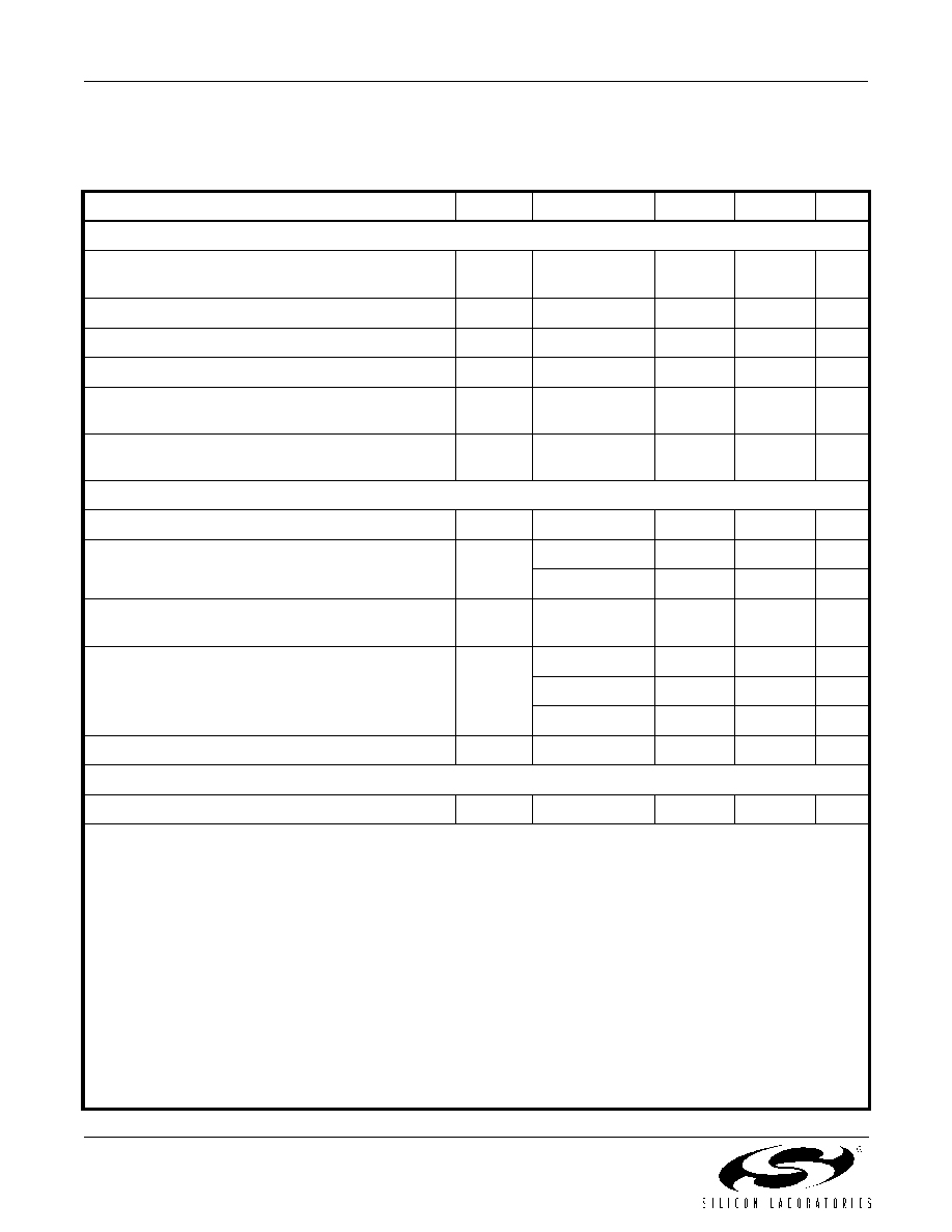
1. Electrical Specifications
Table 1. Absolute Maximum Ratings and Thermal Information1
Parameter
Symbol
Test Condition
Min
Max
Unit
Si3220/Si3225
Supply Voltage
VDD1-
VDD4
–0.5
6.0
V
STIPAC, STIPDC, SRINGAC, SRINGDC Current
–20
+20
mA
Input Current, Digital Pins
IIN
–10
+10
mA
Input Voltage, Digital Pins
VIND
–0.3
VDDD+0.3
V
Analog Ground Differential Voltage
(GND1 to ePad, GND2 to ePad or GND1 to GND2)2
V
GNDA
–50
+50
mV
Digital Ground Differential Voltage
(GND3 to GND4)2
V
GNDD
–50
+50
mV
Si3200
Supply Voltage
VDD
–0.5
6.0
V
High Battery Supply Voltage3
VBATH
Continuous
–104
0.4
V
10 ms
–109
0.4
V
Low Battery Supply Voltage
VBAT,
VBATL
Continuous
VBATH
0.4
V
TIP or RING Voltage
VTIP,
VRING
Continuous
–104
0.4
V
Pulse < 10 us
VBATH–15
0.4
V
Pulse < 4 us
VBATH–35
0.4
V
TIP or RING Current
ITIP, IRING
–100
+100
mA
Si3202
Supply Voltage
VDD
–0.5
6.0
V
Notes:
1. Permanent device damage may occur if the absolute maximum ratings are exceeded, and exposure to absolute
maximum rating conditions for extended periods may affect device reliability. Functional operation should be restricted
to the conditions as specified in the operational sections of this data sheet.
2. The PCB pad placed under the device package must be connected with multiple vias to the PCB ground layer and to
the GND1-GND4 pins via short traces. The TQFP-64 e-Pad must be properly soldered to the PCB pad during PCB
assembly. This type of low-impedance grounding arrangement is necessary to ensure that maximum differentials are
not exceeded under any operating condition in addition to providing thermal dissipation.
3. On Si3200 revision E, the dv/dt of the voltage applied to the VBAT, VBATH, and VBATL pins must be limited to 10 V/s.
4. Operation of the Si3220/Si3225 above 125
C junction temperature may degrade device reliability. The Si3200/Si3202
should be operated at a junction temperature below 140
C for optimal reliability.
5. The thermal resistance of an exposed pad package is assured when the recommended printed circuit board layout
guidelines are followed correctly. The specified performance requires that the exposed pad be soldered to an exposed
copper surface of equal size and that multiple vias are added to enable heat transfer between the top-side copper
surface and a large internal copper ground plane. Refer to “AN55: Dual ProSLIC User Guide” or to the Si3220/3225
evaluation board data sheet for specific layout examples.
相关PDF资料 |
PDF描述 |
|---|---|
| H1KXH-6436M | IDC CABLE - HPK64H/AE64M/X |
| A3BRB-2418M | IDC CABLE - ASR24B/AE24M/APR24B |
| SI3232PPTX-EVB | BOARD EVAL W/DISCRETE INTERFACE |
| SI3216MDCQX-EVB | DAUGHTER CARD W/DISCRETE INTRFC |
| M3TTK-3418J | IDC CABLE - MSD34K/MC34G/MSD34K |
相关代理商/技术参数 |
参数描述 |
|---|---|
| SI3220DCX-EVB | 功能描述:子卡和OEM板 Si3220 Daughter Card RoHS:否 制造商:BeagleBoard by CircuitCo 产品:BeagleBone LCD4 Boards 用于:BeagleBone - BB-Bone - Open Source Development Kit |
| SI3220-F-GQ | 制造商:Silicon Laboratories Inc 功能描述:DUAL-CHANNEL SLIC/CODEC WITH INTERNAL 65 VRMS BALANCED RINGI - Trays |
| SI3220-F-GQR | 制造商:Silicon Laboratories Inc 功能描述:DUAL-CHANNEL SLIC/CODEC WITH INTERNAL 65 VRMS BALANCED RINGI - Tape and Reel |
| Si3220-FQ | 功能描述:电信线路管理 IC Dual-Channel SLIC/ codec RoHS:否 制造商:STMicroelectronics 产品:PHY 接口类型:UART 电源电压-最大:18 V 电源电压-最小:8 V 电源电流:30 mA 最大工作温度:+ 85 C 最小工作温度:- 40 C 安装风格:SMD/SMT 封装 / 箱体:VFQFPN-48 封装:Tray |
| SI3220-FQR | 制造商:Silicon Laboratories Inc 功能描述: 制造商:Silicon Laboratories Inc 功能描述:SLIC 2CH 63DB 45MA 3.3V/5V 64TQFP - Tape and Reel |
发布紧急采购,3分钟左右您将得到回复。