- 您现在的位置:买卖IC网 > PDF目录10727 > SI4136-F-GM (Silicon Laboratories Inc)IC SYNTHESIZER RF1/RF2/IF 28QFN PDF资料下载
参数资料
| 型号: | SI4136-F-GM |
| 厂商: | Silicon Laboratories Inc |
| 文件页数: | 10/34页 |
| 文件大小: | 0K |
| 描述: | IC SYNTHESIZER RF1/RF2/IF 28QFN |
| 标准包装: | 60 |
| 类型: | * |
| 驱动器/接收器数: | * |
| 规程: | * |
| 电源电压: | 2.7 V ~ 3.6 V |
| 安装类型: | 表面贴装 |
| 封装/外壳: | 28-VFQFN 裸露焊盘 |
| 供应商设备封装: | 28-QFN(5x5) |
| 包装: | 管件 |
| 产品目录页面: | 585 (CN2011-ZH PDF) |
| 其它名称: | 336-1178 |
第1页第2页第3页第4页第5页第6页第7页第8页第9页当前第10页第11页第12页第13页第14页第15页第16页第17页第18页第19页第20页第21页第22页第23页第24页第25页第26页第27页第28页第29页第30页第31页第32页第33页第34页
Si4136/Si4126
18
Rev. 1.41
programmed independently. Programming either the R-
or N-Divider register for RF1 or RF2 automatically
selects the associated output.
When XINDIV2 = 0, the reference frequency on the XIN
pin is divided by R and this signal is the input to the
PLL’s phase detector. The other input to the phase
detector is the PLL’s VCO output frequency divided by
2N for the RF PLLs or N for the IF PLL. After an initial
transient
Equation 1. fOUT = (2N/R) fREF (for the RF PLLs)
Equation 2. fOUT = (N/R) fREF (for the IF PLL).
The integers R are set by programming the RF1 R-
Divider register (Register 6), the RF2 R-Divider register
(Register 7) and the IF R-Divider register (Register 8).
The integers N are set by programming the RF1 N-
Divider register (register 3), the RF2 N-Divider register
(Register 4), and the IF N-Divider register (Register 5).
If the optional divide-by-2 circuit on the XIN pin is
enabled (XINDIV2 = 1) then after an initial transient
fOUT = (N/R) fREF (for the RF PLLs)
fOUT = (N/2R) fREF (for the IF PLL).
Each N-Divider is implemented as a conventional high
speed divider. That is, it consists of a dual-modulus
prescaler, a swallow counter, and a lower speed
synchronous counter. However, the control of these
sub-circuits
is
handled
automatically.
Only
the
appropriate N value should be programmed.
2.5. PLL Loop Dynamics
The transient response for each PLL is determined by
its phase detector update rate f (equal to fREF/R) and
the phase detector gain programmed for each RF1,
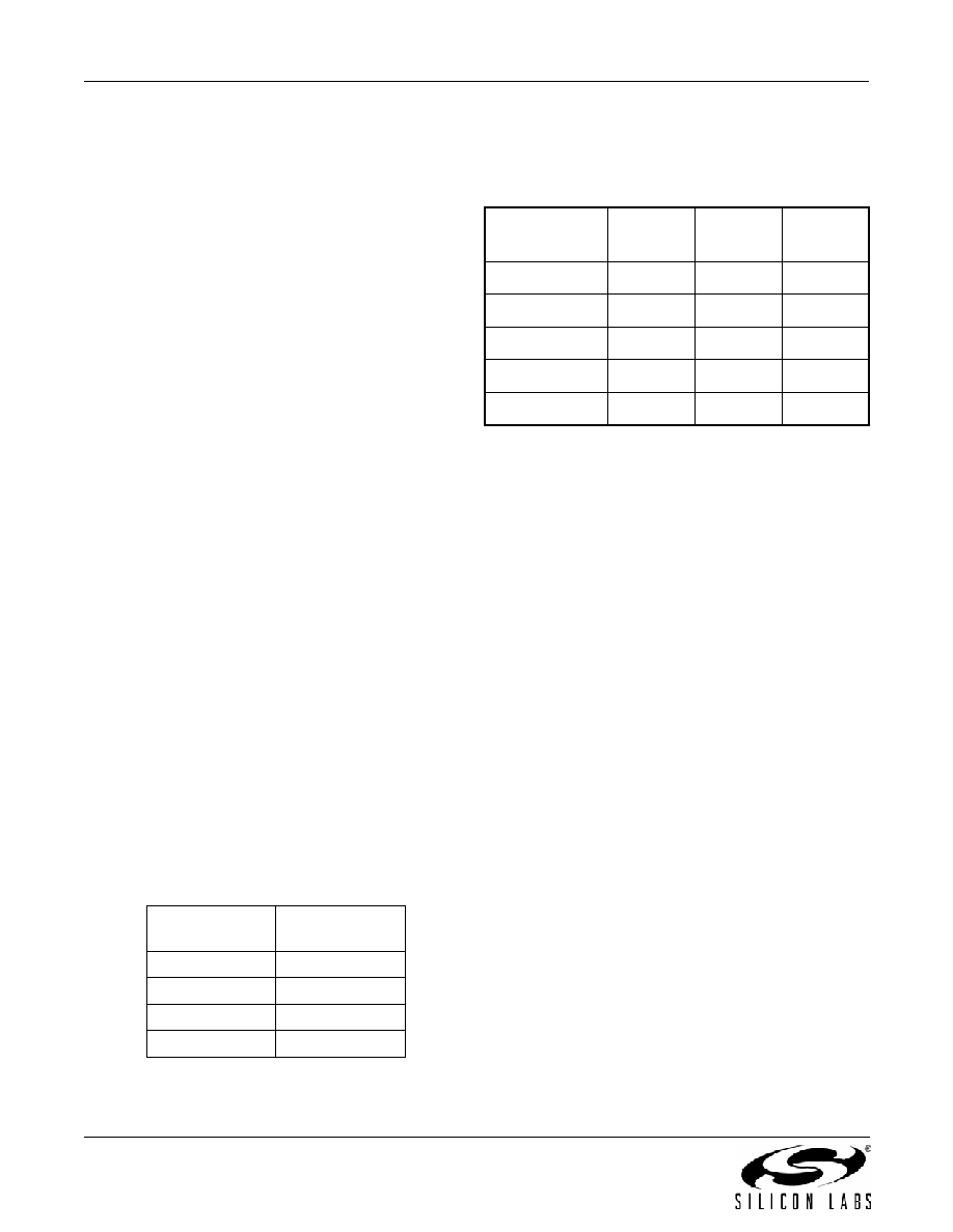
RF2, or IF synthesizer. (See Register 1.) Four different
settings for the phase detector gain are available for
each PLL. The highest gain is programmed by setting
the two phase detector gain bits to 00, and the lowest by
setting the bits to 11. The values of the available gains,
relative to the highest gain, are listed in Table 7.
In general, a higher phase detector gain will decrease
in-band phase noise and increase the speed of the PLL
transient until the point at which stability begins to be
compromised. The optimal gain depends on N. Table 8
lists recommended settings for different values of N.
The VCO gain and loop filter characteristics are not
programmable.
The settling time for each PLL is directly proportional to
its phase detector update period T (T equals 1/f).
During the first 13 update periods the Si4136 executes
the self-tuning algorithm. Thereafter the PLL controls
the
output
frequency.
Because
of
the
unique
architecture of the Si4136 PLLs, the time required to
settle the output frequency to 0.1 ppm error is only
about 25 update periods. Thus, the total time after
power-up or a change in programmed frequency until
the synthesized frequency is well settled—including
time for self-tuning—is around 40 update periods.
Note: This settling time analysis holds for f 500 kHz. For
f 500 kHz, the settling time can be a maximum of
100
s as specified in Table 5.
2.6. RF and IF Outputs (RFOUT and IFOUT)
The RFOUT and IFOUT pins are driven by amplifiers
that buffer the RF VCOs and IF VCO, respectively. The
RF output amplifier receives its input from either the
RF1 or RF2 VCO, depending upon which R- or N-
Divider
register
was
last
written.
For
example,
programming
the
N-Divider
register
for
RF1
automatically selects the RF1 VCO output.
Figure 13 on page 15 shows an application diagram for
the Si4136. The RF output signal must be AC coupled
to its load through a capacitor.
The IFOUT pin must also be AC coupled to its load
through a capacitor. The IF output level is dependent
upon the load. Figure 17 displays the output level
versus load resistance. For resistive loads greater than
500
the output level saturates and the bias currents in
the IF output amplifier are higher than they need to be.
The LPWR bit in the Main Configuration register
Table 7. Gain Values (Register 1)
KP Bits
Relative P.D.
Gain
00
1
01
1/2
10
1/4
11
1/8
Table 8. Optimal KP Settings
N
RF1
KP1<1:0>
RF2
KP2<1:0>
IF
KPI<1:0>
2047
00
2048 to 4095
00
01
4096 to 8191
01
10
8192 to 16383
10
11
16384
11
相关PDF资料 |
PDF描述 |
|---|---|
| VI-J62-MY-F3 | CONVERTER MOD DC/DC 15V 50W |
| MCP3424-E/SL | IC ADC 18BIT 3.75SPS 4CH 14-SOIC |
| MCP3208-CI/P | IC ADC 12BIT 2.7V 8CH SPI 16-DIP |
| MCP3208-CI/SL | IC ADC 12BIT 2.7V 8CH SPI 16SOIC |
| VI-J4Y-MW-F1 | CONVERTER MOD DC/DC 3.3V 66W |
相关代理商/技术参数 |
参数描述 |
|---|---|
| SI4136-F-GMR | 功能描述:时钟发生器及支持产品 WLAN Satellite Radio Synthesizer RoHS:否 制造商:Silicon Labs 类型:Clock Generators 最大输入频率:14.318 MHz 最大输出频率:166 MHz 输出端数量:16 占空比 - 最大:55 % 工作电源电压:3.3 V 工作电源电流:1 mA 最大工作温度:+ 85 C 安装风格:SMD/SMT 封装 / 箱体:QFN-56 |
| SI4136-F-GT | 功能描述:射频无线杂项 WLAN SATELITE RADIO TSSOP-24 RoHS:否 制造商:Texas Instruments 工作频率:112 kHz to 205 kHz 电源电压-最大:3.6 V 电源电压-最小:3 V 电源电流:8 mA 最大功率耗散: 工作温度范围:- 40 C to + 110 C 封装 / 箱体:VQFN-48 封装:Reel |
| SI4136-F-GTR | 功能描述:射频无线杂项 WLAN Satellite Radio Synthesizer RoHS:否 制造商:Texas Instruments 工作频率:112 kHz to 205 kHz 电源电压-最大:3.6 V 电源电压-最小:3 V 电源电流:8 mA 最大功率耗散: 工作温度范围:- 40 C to + 110 C 封装 / 箱体:VQFN-48 封装:Reel |
| SI4136M-EVB | 功能描述:开发板和工具包 - 无线 802.11b and ISM Band RoHS:否 制造商:Arduino 产品:Evaluation Boards 工具用于评估:AT32UC3L 核心:AVR32 频率: 接口类型:USB 工作电源电压:5 V |
| SI4154DY | 制造商:VISHAY 制造商全称:Vishay Siliconix 功能描述:N-Channel 40-V (D-S) MOSFET |
发布紧急采购,3分钟左右您将得到回复。