参数资料
| 型号: | SI5017-EVB |
| 厂商: | Silicon Laboratories Inc |
| 文件页数: | 2/12页 |
| 文件大小: | 0K |
| 描述: | BOARD EVALUATION FOR SI5017 |
| 标准包装: | 1 |
| 主要目的: | 计时,时钟和数据恢复(CDR) |
| 已用 IC / 零件: | SI5017 |
| 已供物品: | 板 |
| 其它名称: | 336-1125 |
�� �
�
�Si5017-EVB�
�Functional� Description�
�The� evaluation� board� simplifies� characterization� of� the�
�Si5017� Clock� and� Data� Recovery� (CDR)� device� by�
�providing� access� to� all� of� the� Si5017� I/Os.� Device�
�performance� can� be� evaluated� by� following� the� “Test�
�Configuration”� section.� Specific� performance� metrics�
�include� input� sensitivity,� jitter� tolerance,� jitter� generation,�
�and� jitter� transfer.�
�Power� Supply�
�The� evaluation� board� requires� one� 3.3� V� supply.� Supply�
�When� applied,� REFCLK� is� used� to� center� the� frequency�
�of� the� DSPLL?� so� the� device� can� lock� to� the� data.�
�Ideally,� the� REFCLK� frequency� should� be� 1/128th,�
�1/32nd,� or� 1/16th� the� VCO� frequency� and� must� have� a�
�frequency� accuracy� of� ±100� ppm.� Internally,� the� CDR�
�automatically� recognizes� the� REFCLK� frequency� within�
�one� of� these� three� frequency� ranges.� Typical� REFCLK�
�frequencies� are� given� in� Table� 1.� REFCLK� is� ac� coupled�
�to� the� SMA� jacks� located� on� the� top� side� of� the�
�evaluation� board.�
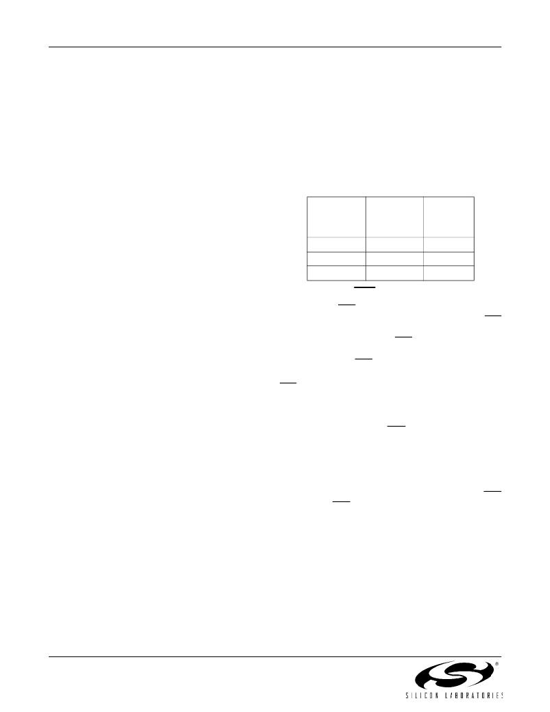
�Table� 1.� Typical� REFCLK� Frequencies�
�filtering� is� placed� on� the� board� to� filter� typical� system�
�noise� components;� however,� initial� performance� testing�
�should� use� a� linear� supply� capable� of� supplying� the�
�nominal� voltage� ±5%� dc.�
�CAUTION� :� The� evaluation� board� is� designed� so� that� the�
�body� of� the� SMA� jacks� and� GND� are� shorted.� Care� must�
�be� taken� when� powering� the� PCB� at� potentials� other�
�than� GND� at� 0.0� V� and� VDD� at� 3.3� V� relative� to� chassis�
�SONET/SDH�
�19.44� MHz�
�77.76� MHz�
�155.52� MHz�
�SONET/SDH�
�with�
�15/14� FEC�
�20.83� MHz�
�83.31� MHz�
�166.63� MHz�
�Ratio� of�
�VCO� to�
�REFCLK�
�128�
�32�
�16�
�V� LOS� =� ---------------------------------------�
�GND.�
�Device� Powerdown�
�The� CDR� can� be� powered� down� via� the� RESET/CAL�
�signal.� When� asserted,� the� evaluation� board� draws�
�minimal� current.� RESET/CAL� is� controlled� via� one�
�jumper� located� in� the� lower� left-hand� corner� of� the�
�evaluation� board.� RESET/CAL� is� wired� to� the� signal�
�post� adjacent� to� the� VDD� post.� For� a� valid� reset� to� occur�
�when� using� external� reference� clock� mode,� a� proper�
�external� reference� clock� frequency� must� be� applied� as�
�specified� in� Table� 1.� CLKOUT,� DATAOUT,� DATAIN�
�CLKOUT,� DATAOUT,� and� DATAIN� (all� high-speed� I/Os)�
�are� wired� to� the� board� perimeter� on� 30� mil� (0.030� inch)�
�50� ?� microstrip� lines� to� the� end-launch� SMA� jacks� as�
�labeled� on� the� PCB.� These� I/Os� are� ac� coupled� to�
�simplify� direct� connection� to� a� wide� array� of� standard�
�test� hardware.� Because� each� of� these� signals� are�
�differential,� both� the� positive� (+)� and� negative� (–)�
�terminals� must� be� terminated� to� 50� ?� .� Terminating� only�
�one� side� will� adversely� degrade� the� performance� of� the�
�CDR.� The� inputs� are� terminated� on� the� die� with� 50� ?�
�resistors.�
�Note:� The� 50� ?� termination� is� for� each� terminal/side� of� a� dif-�
�ferential� signal,� thus� the� differential� termination� is� actu-�
�ally� 50� ?� +� 50� ?� =� 100� ?� .�
�REFCLK�
�REFCLK� is� optional� for� clock� and� data� recovery� within�
�the� Si5017� device.� If� REFCLK� is� not� used,� jumper� both�
�JP15� and� JP16.� These� jumpers� pull� the� REFCLK+� input�
�to� VDD� and� REFCLK–� input� to� GND,� which� configures�
�the� device� to� operate� without� an� external� reference.�
�Loss-of-Lock� (LOL)�
�Loss-of-lock� (LOL)� is� an� indicator� of� the� relative�
�frequency� between� the� data� and� the� REFCLK.� LOL�
�asserts� when� the� frequency� difference� is� greater� than�
�±600� ppm.� To� prevent� LOL� from� de-asserting�
�prematurely,� there� is� hysterisis� in� returning� from� the� out-�
�of-lock� condition.� LOL� will� be� de-asserted� when� the�
�frequency� difference� is� less� than� ±300� ppm.�
�LOL� is� wired� to� a� test� point� which� is� located� on� the�
�upper� right-hand� side� of� the� evaluation� board.�
�Loss-of-Signal� Alarm� Threshold� Control�
�The� loss-of-signal� alarm� (LOS)� is� used� to� signal� low�
�incoming� data� amplitude� levels.� The� programmable�
�threshold� control� is� set� by� applying� a� dc� voltage� level�
�from� a� low� noise� voltage� source� to� the� LOS_LVL� pin.�
�The� LOS_LVL� is� controllable� through� the� BNC� jack� J10.�
�The� mapping� of� the� LOS_LVL� voltage� to� input� signal�
�alarm� threshold� level� is� shown� in� Figure� 1.� The� LOS�
�Threshold� to� LOS� Level� is� mapped� as� follows:�
�V� LOS_LVL� –� 1.5�
�25�
�If� this� function� is� not� used,� install� jumper� to� JP1� header.�
�2�
�Rev.� 1.0�
�相关PDF资料 |
PDF描述 |
|---|---|
| SI5018-EVB | BOARD EVALUATION FOR SI5018 |
| SI5020-EVB | BOARD EVALUATION FOR SI5020 |
| SI5023-EVB | BOARD EVALUATION FOR SI5023 |
| SI5110-EVB | BOARD EVALUATION FOR SI5110 |
| SI5320-EVB | BOARD EVALUATION FOR SI5320 |
相关代理商/技术参数 |
参数描述 |
|---|---|
| SI5017-X-GM | 制造商:SILABS 制造商全称:SILABS 功能描述:OC-48/STM-16 SONET/SDH CDR IC WITH LIMITING AMPLIFIER |
| SI5018 | 制造商:SILABS 制造商全称:SILABS 功能描述:SiPHY⑩ OC-48/STM-16 CLOCK AND DATA RECOVERY IC WITH FEC |
| SI-50182 | 制造商:BEL 制造商全称:Bel Fuse Inc. 功能描述:SI-50182 |
| SI-50183 | 制造商:BEL 制造商全称:Bel Fuse Inc. 功能描述:SI-50183 |
| SI-50184 | 制造商:BEL 制造商全称:Bel Fuse Inc. 功能描述:SI-50184 |
发布紧急采购,3分钟左右您将得到回复。