- 您现在的位置:买卖IC网 > PDF目录16488 > SI5100-EVB (Silicon Laboratories Inc)BOARD EVALUATION FOR SI5100 PDF资料下载
参数资料
| 型号: | SI5100-EVB |
| 厂商: | Silicon Laboratories Inc |
| 文件页数: | 5/48页 |
| 文件大小: | 0K |
| 描述: | BOARD EVALUATION FOR SI5100 |
| 标准包装: | 1 |
| 主要目的: | 接口,SONET/SDH,收发器 |
| 已用 IC / 零件: | SI5100 |
| 已供物品: | 主板和子卡组套 |
| 其它名称: | 336-1136 |
第1页第2页第3页第4页当前第5页第6页第7页第8页第9页第10页第11页第12页第13页第14页第15页第16页第17页第18页第19页第20页第21页第22页第23页第24页第25页第26页第27页第28页第29页第30页第31页第32页第33页第34页第35页第36页第37页第38页第39页第40页第41页第42页第43页第44页第45页第46页第47页第48页
�� �
�
�Si5100/Si5110-EVB�
�Functional� Description�
�The� Si5100-EVB� and� Si5110-EVB� motherboard� and�
�daughter� card� sets� simplify� characterization� of� the� OC-�
�48/STM-16� and� FEC� transceiver� devices� by� providing�
�Data� I/O� Signals�
�The� serial� 2.5� Gbps� data� and� 2.5� GHz� clock� paths� are�
�routed� as� coplanar� differentially-coupled� microstrip�
�transmission� lines� on� the� daughter� card.� These� three�
�convenient� access� to�
�the� device� I/Os.� Device�
�signals� (RXDIN,� TXCLKOUT,� and� TXDOUT)� are� ac�
�performance� can� be� evaluated� in� various� modes� by�
�following� the� “Basic� Test� Setup”� section.�
�Power� Supply�
�The� transceiver� device� can� be� powered� from� a� single�
�1.8� V� supply� or� seperate� 1.8� V� and� 3.3� V� supplies.�
�When� the� additional� 3.3� V� supply� is� applied,� the� status�
�outputs� are� LVTTL� compatible.� The� daughter� card� can�
�be� configured� for� either� mode� of� operation� by� setting� the�
��For� 3.3� V/1.8� V� operation�
�coupled� to� standard� SMA� jacks� for� ease� in� connection�
�to� industry� standard� test� equipment.� Take� care� when�
�connecting� cables� to� these� jacks.� Use� a� standard� SMA�
�torque� wrench� to� minimize� reflections� at� the� cable-to-�
�jack� interface.� Finally,� match� all� differential� connections�
�in� length� to� minimize� phase� differences� between� the�
�positive� and� negative� terminals.�
�Differential� Parallel� Data� and�
�Clock� I/O� Signals�
�The� differential� parallel� data� lines� are� routed� through� the�
�300-pin� meg-array� connector� to� the� motherboard.� The�
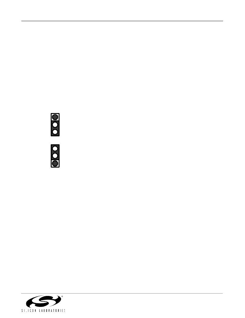
�VDD_IO�
�SEL�
�1.8� V�
�3.3� V�
�standard� loopback� motherboard� directly� couples� the�
�RXDOUT� bus� to� the� TXDIN� bus.� The� optional� full-�
�duplex� motherboard� directly� couples� the� RXDOUT� and�
�TXDIN� buses� to� standard� SMA� jacks� for� connection� to�
�industry� standard� test� equipment.�
�For� 1.8� V� operation� only�
�Slice� Level,� Loss-of-Signal� Level,� and�
�VDD_IO�
�SEL�
�1.8� V�
�Phase� Adjust�
�Voltages� present� at� the� Slice� Level� (SLICELVL),� Loss-�
�of-Signal� Level� (LOSLVL)� and� Phase� Adjust�
�3.3� V�
�Figure� 4.� VDD_IO� Selection� Jumpers�
�Control� Inputs�
�The� device� control� inputs� are� located� on� the�
�motherboard� and� daughter� card.� Signals� with� equivalent�
�module� functions� are� routed� to� the� motherboard� header,�
�JP1.� Signals� specific� to� the� transceiver� are� routed� on�
�the� daughter� card� to� jumpers� JP1� and� JP2.� In� both�
�cases,� the� signal� is� routed� to� the� center� pin� of� a� three�
�pin� group� where� the� adjacent� pins� are� power� and�
�ground.� The� device� inputs� are� pulled� high� or� low� so� that�
�leaving� a� signal� unconnected� will� not� harm� the� device.�
�Status� Outputs�
�The� device� status� outputs� are� located� on� the�
�motherboard� and� daughter� card.� Signals� with� equivalent�
�module� functions� are� routed� to� the� motherboard� header,�
�JP2.� Signals� specific� to� the� transceiver� are� routed� on�
�the� daughter� card� to� headers� JP3� and� JP4.� In� both�
�cases,� the� signal� is� routed� to� a� header� pin� adjacent� to� a�
�ground� pin.�
�(PHASEADJ)� pins� can� be� used� to� adjust� the� data� slicing�
�level,� the� loss-of-signal� alarm� level,� and� the� sampling�
�phase� position,� respectively.� Because� these� inputs� are�
�high� impedance,� simple� turn-based� potentiometers� are�
�used� to� apply� the� control� voltage.� The� Si5100-EVB�
�provides� 50� k� ?� potentiometers� for� each� of� these� inputs:�
�potentiometer� R16� sets� the� voltage� applied� to� the�
�SLICELVL� pin;� R14� sets� the� voltage� applied� to� the�
�LOSLVL� pin,� and� R15� sets� the� voltage� applied� to� the�
�PHASEADJ� pin.� The� Si5110-EVB� also� provides� 50� k� ?�
�potentiometers� for� each� of� these� inputs.� Potentiometer�
�R5� sets� the� voltage� applied� to� the� SLICELVL� pin;� R3�
�sets� the� voltage� applied� to� the� LOSLVL� pin,� and� R4� sets�
�the� voltage� applied� to� the� PHASEADJ� pin.� The�
�potentiometers� are� connected� so� the� voltage� applied�
�varies� from� GND� to� VREF.� Refer� to� the� device� data�
�sheet� for� details� on� the� operation� of� these� inputs.�
�Basic� Test� Setup�
�The� configurations� listed� in� Tables� 1� and� 3� allow� easy�
�setup� of� the� transceiver� evaluation� system� for� operation�
�in� the� line� loopback,� full� duplex,� or� diagnostic� loopback�
�modes.� Other� configurations� are� supported;� however,�
�operation� should� first� be� verified� in� one� of� these� modes�
�in� order� to� minimize� the� number� of� unknown� variables.�
�Preliminary� Rev.� 0.5�
�5�
�相关PDF资料 |
PDF描述 |
|---|---|
| AFK336M80F24T-F | CAP ALUM 33UF 80V 20% SMD |
| 1-6278027-2 | C/A ST/MT-RJ, MM 2FT |
| XR16M570IL24-0B-EB | EVAL BOARD FOR XR16M570-B 24QFN |
| SPD73R-103M | INDUCTOR PWR SHIELDED 10UH SMD |
| 1906015-8 | CA 2.0MM OFNR 50/125,LC SEC GRN |
相关代理商/技术参数 |
参数描述 |
|---|---|
| SI5100-F-BC | 功能描述:电信线路管理 IC SONET/SDH Trnscvr RoHS:否 制造商:STMicroelectronics 产品:PHY 接口类型:UART 电源电压-最大:18 V 电源电压-最小:8 V 电源电流:30 mA 最大工作温度:+ 85 C 最小工作温度:- 40 C 安装风格:SMD/SMT 封装 / 箱体:VFQFPN-48 封装:Tray |
| SI5100-G-BC | 功能描述:电信线路管理 IC OC-48 STM-16 SONET SDH TRANSCEIVER RoHS:否 制造商:STMicroelectronics 产品:PHY 接口类型:UART 电源电压-最大:18 V 电源电压-最小:8 V 电源电流:30 mA 最大工作温度:+ 85 C 最小工作温度:- 40 C 安装风格:SMD/SMT 封装 / 箱体:VFQFPN-48 封装:Tray |
| Si5100-H-BL | 功能描述:电信线路管理 IC OC-48 STM-16 SONET SDH Trnscvr 1:16 RoHS:否 制造商:STMicroelectronics 产品:PHY 接口类型:UART 电源电压-最大:18 V 电源电压-最小:8 V 电源电流:30 mA 最大工作温度:+ 85 C 最小工作温度:- 40 C 安装风格:SMD/SMT 封装 / 箱体:VFQFPN-48 封装:Tray |
| Si5100-H-GL | 功能描述:电信线路管理 IC OC-48 STM-16 SONET SDH Trnscvr 1:16 RoHS:否 制造商:STMicroelectronics 产品:PHY 接口类型:UART 电源电压-最大:18 V 电源电压-最小:8 V 电源电流:30 mA 最大工作温度:+ 85 C 最小工作温度:- 40 C 安装风格:SMD/SMT 封装 / 箱体:VFQFPN-48 封装:Tray |
| SI-51010-F | 制造商:Bel Fuse 功能描述:- Trays |
发布紧急采购,3分钟左右您将得到回复。