- 您现在的位置:买卖IC网 > PDF目录16215 > SI5310-EVB (Silicon Laboratories Inc)BOARD EVALUATION FOR SI5310 PDF资料下载
参数资料
| 型号: | SI5310-EVB |
| 厂商: | Silicon Laboratories Inc |
| 文件页数: | 4/26页 |
| 文件大小: | 0K |
| 描述: | BOARD EVALUATION FOR SI5310 |
| 标准包装: | 1 |
| 主要目的: | 计时,时钟发生器 |
| 已用 IC / 零件: | SI5310 |
| 已供物品: | 板 |
| 其它名称: | 336-1140 |
Si5310
12
Rev. 1.3
4. Functional Description
The Si5310 is an integrated clock multiplier and clock
regenerator device based on SIlicon Laboratories
DSPLL technology. The DSPLL phase locks to the
clock input signal (CLKIN) and generates a phase-
locked output clock (MULTOUT) at a multiple of the
input clock frequency. The DSPLL is also employed to
regenerate an output clock (CLKOUT) that is a jitter-
attenuated version of the input clock with clean rising
and falling edges.
The MULTOUT output is configured to operate in either
the 150–167 MHz or the 600–668 MHz frequency range
using the MULTSEL control input. A reference clock
input signal (REFCLK) is used by the DSPLL as a
reference for determination of the PLL lock status. For
convenience, REFCLK can be provided at any one of
five frequencies, each a multiple of the CLKIN
frequency. The REFCLK rate is automatically detected,
so no control inputs are needed for configuration. The
REFCLK input can be synchronous or asynchronous
with respect to the CLKIN input. The operating ranges
for the CLKIN, CLKOUT, MULTOUT, and REFCLK
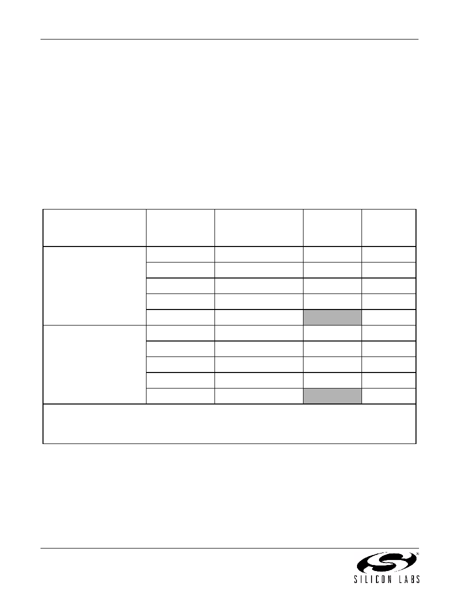
signals are indicated in Table 9. Typical values for
several applications are presented in Table 10.
Table 9. CLKIN, CLKOUT, MULTOUT, REFCLK Operating Ranges
MULTSEL
CLKIN Range
(MHz)
REFCLK = 2n x CLKIN
±100 ppm
(See Note 1)
CLKOUT
MULTOUT
0
(MULTOUT = 600–668 MHz)
37.500–41.750
n = –2, –1, 0, 1, 2
1xCLKIN
16xCLKIN
75.000–83.500
n = –3, –2, –1, 0, 1
1xCLKIN
8xCLKIN
150.000–167.000
n = –4, –3, –2, –1, 0
1xCLKIN
4xCLKIN
300.000–334.000
n = –5, –4, –3, –2, –1
1xCLKIN
2xCLKIN
600.000–668.000
n = –6, –5, –4, –3, –2
See Note 2
1xCLKIN
1
(MULTOUT = 150–167 MHz)
9.375–10.438
n = 0, 1, 2, 3, 4
1xCLKIN
16xCLKIN
18.750–20.875
n = –1, 0, 1, 2, 3
1xCLKIN
8xCLKIN
37.500–41.750
n = –2, –1, 0, 1, 2
1xCLKIN
4xCLKIN
75.000–83.500
n = –3, –2, –1, 0, 1
1xCLKIN
2xCLKIN
150.000–167.000
n = –4, –3, –2, –1, 0
See Note 2
1xCLKIN
Note:
1. The REFCLK input can be set to any one of the five CLKIN multiples indicated. The REFCLK input can be
asynchronous to the CLKIN input, but must be within ±100 ppm of the stated CLKIN multiple.
2. The CLKOUT output is not valid for MULTOUT:CLKIN ratios of 1:1 (MULTOUT = 1 x CLKIN.)
相关PDF资料 |
PDF描述 |
|---|---|
| ASM06DRSH-S288 | CONN EDGECARD 12POS .156 EXTEND |
| RBM08DCCT-S189 | CONN EDGECARD 16POS R/A .156 SLD |
| RBM08DCBT-S189 | CONN EDGECARD 16POS R/A .156 SLD |
| RBM08DCAT-S189 | CONN EDGECARD 16POS R/A .156 SLD |
| GCM18DSEN-S13 | CONN EDGECARD 36POS .156 EXTEND |
相关代理商/技术参数 |
参数描述 |
|---|---|
| SI5310-GM | 功能描述:锁相环 - PLL Clock Multiplier Regenerator RoHS:否 制造商:Silicon Labs 类型:PLL Clock Multiplier 电路数量:1 最大输入频率:710 MHz 最小输入频率:0.002 MHz 输出频率范围:0.002 MHz to 808 MHz 电源电压-最大:3.63 V 电源电压-最小:1.71 V 最大工作温度:+ 85 C 最小工作温度:- 40 C 封装 / 箱体:QFN-36 封装:Tray |
| SI5310-GMR | 制造商:Silicon Laboratories Inc 功能描述: |
| SI5311 | 制造商:未知厂家 制造商全称:未知厂家 功能描述:PRECISION HIGH SPEED CLOCK MULTIPLIER/REGENERATOR IC |
| SI53112-A00AGM | 功能描述:IC BUFFER ZDB PCIE 1:12 64-QFN 制造商:silicon labs 系列:- 包装:托盘 零件状态:有效 PLL:是 主要用途:Intel QPI,PCI Express(PCIe) 输入:时钟 输出:HCSL 电路数:1 比率 - 输入:输出:1:12 差分 - 输入:输出:是/是 频率 - 最大值:133.33MHz 电压 - 电源:3.135 V ~ 3.465 V 工作温度:-40°C ~ 85°C 安装类型:表面贴装 封装/外壳:64-VFQFN 裸露焊盘 供应商器件封装:64-QFN(9x9) 标准包装:260 |
| SI53112-EK | 功能描述:Si53112 - Timing, Clock Buffer Evaluation Board 制造商:silicon labs 系列:- 零件状态:有效 主要用途:计时,时钟缓冲器 嵌入式:- 使用的 IC/零件:Si53112 主要属性:- 辅助属性:- 所含物品:板 标准包装:1 |
发布紧急采购,3分钟左右您将得到回复。