- 您现在的位置:买卖IC网 > PDF目录9191 > SI5317B-C-GM (Silicon Laboratories Inc)IC CLK JITTER CLEANR PROG 36QFN PDF资料下载
参数资料
| 型号: | SI5317B-C-GM |
| 厂商: | Silicon Laboratories Inc |
| 文件页数: | 6/46页 |
| 文件大小: | 0K |
| 描述: | IC CLK JITTER CLEANR PROG 36QFN |
| 应用说明: | SI5315/17 Crystal Selection AppNote |
| 特色产品: | Si5317 Jitter Cleaning Clock |
| 标准包装: | 490 |
| 系列: | DSPLL® |
| 类型: | 抖动消除器 |
| PLL: | 带旁路 |
| 输入: | 时钟,晶体 |
| 输出: | CML,CMOS,LVDS,LVPECL |
| 电路数: | 1 |
| 比率 - 输入:输出: | 1:2 |
| 差分 - 输入:输出: | 是/是 |
| 频率 - 最大: | 350MHz |
| 除法器/乘法器: | 无/无 |
| 电源电压: | 1.71 V ~ 3.63 V |
| 工作温度: | -40°C ~ 85°C |
| 安装类型: | 表面贴装 |
| 封装/外壳: | 36-VFQFN 裸露焊盘 |
| 供应商设备封装: | 36-QFN(6x6) |
| 包装: | 托盘 |
| 产品目录页面: | 628 (CN2011-ZH PDF) |
| 其它名称: | 336-1922 |
第1页第2页第3页第4页第5页当前第6页第7页第8页第9页第10页第11页第12页第13页第14页第15页第16页第17页第18页第19页第20页第21页第22页第23页第24页第25页第26页第27页第28页第29页第30页第31页第32页第33页第34页第35页第36页第37页第38页第39页第40页第41页第42页第43页第44页第45页第46页
Si5317
14
Rev. 1.1
2. Functional Description
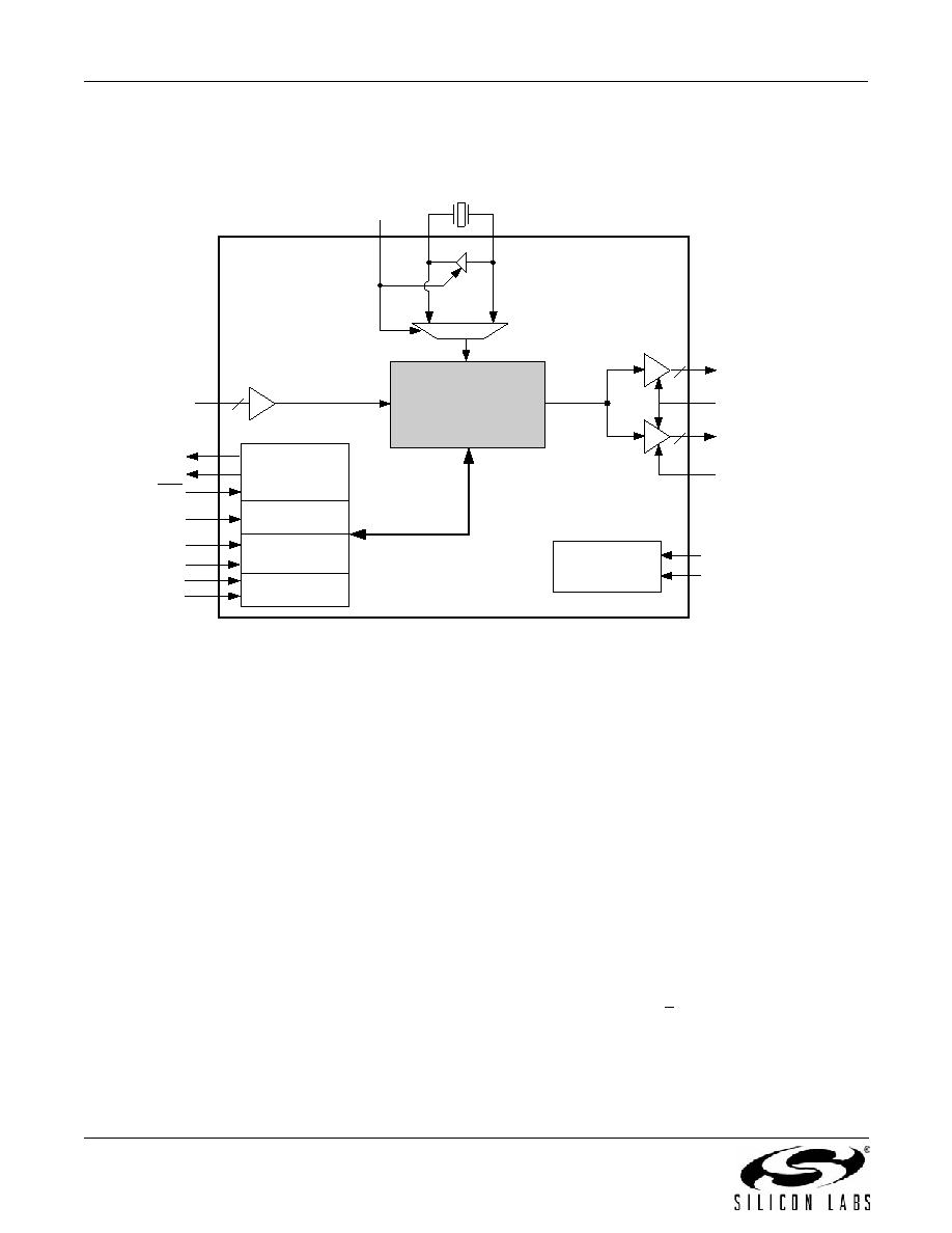
Figure 5. Detailed Block Diagram
2.1. Overview
The Si5317 is a 1:1 jitter-attenuating precision clock for applications requiring sub 1 ps jitter performance. The
Si5317 accepts one clock input ranging from 1 to 711 MHz and generates two clock outputs at the same frequency
ranging from 1 to 711 MHz. The Si5317 is based on Silicon Laboratories' 3rd-generation DSPLL technology,
which provides jitter attenuation on any frequency in a highly integrated PLL solution that eliminates the need for
external VCXO and loop filter components. The nominal operating frequency is selectable from a look-up table.
The Si5317 PLL loop bandwidth (BW) is selectable via the BWSEL[1:0] pins and supports a range from 60 Hz to
8.4 kHz.
The Si5317 monitors the input clock for loss-of-signal (LOS) and provides a LOS alarm when it detects missing
pulses on the input clock. The device monitors the lock status of the DSPLL. The lock detect algorithm works by
continuously monitoring the phase of the input clock in relation to the phase of the feedback clock.
The Si5317 provides a VCO freeze capability that allows the device to continue generation of a stable output clock
when the selected input clock is lost. During VCO freeze, the DSPLL latches its VCO settings and uses its XA/XB
clock as its frequency reference.
The Si5317 has two output clock drivers and can be configured as four single-ended or two differential outputs.
The signal format of the clock output is selectable to support LVPECL, LVDS, CML, or CMOS loads. The device
operates from a single 1.8, 2.5, or 3.3 V supply. The use of LVPECL requires a VDD > 2.25 V.
DSPLL
LOS
LOL
BWSEL[1:0]
CKIN+
CKIN–
CKOUT+
CKOUT–
VDD (1.8, 2.5, or 3.3 V)
GND
2
FRQSEL[3:0]
RST
RATE[1:0]
XA
XB
fOSC
2
f3
Frequency
Control
Bandwidth
Control
Alarms
Control
External Crystal or
Reference Clock
FRQTBL
Voltage
Regulator with
High PSRR
SFOUT[1:0]
2
CKOUT+
CKOUT–
Skew Control
INC
DEC
DBL2_BY
相关PDF资料 |
PDF描述 |
|---|---|
| X9251TS24IZ | IC XDCP QUAD 256TAP 100K 24-SOIC |
| VI-2WZ-MX-F1 | CONVERTER MOD DC/DC 2V 30W |
| VI-2WZ-MW-F4 | CONVERTER MOD DC/DC 2V 40W |
| X9408YV24IZ-2.7 | IC XDCP QUAD 64TAP 10K 24-TSSOP |
| SI5338C-A-GM | IC CLK GEN QUAD 200MHZ 24-QFN |
相关代理商/技术参数 |
参数描述 |
|---|---|
| SI5317B-C-GMR | 功能描述:时钟合成器/抖动清除器 Pin-Program Jitter Clean Clk 1In/2Out RoHS:否 制造商:Skyworks Solutions, Inc. 输出端数量: 输出电平: 最大输出频率: 输入电平: 最大输入频率:6.1 GHz 电源电压-最大:3.3 V 电源电压-最小:2.7 V 封装 / 箱体:TSSOP-28 封装:Reel |
| Si5317C-C-GM | 功能描述:标准时钟振荡器 Pin-Program. Jitter Cleaning Clock RoHS:否 制造商:AVX 产品:Standard Clock Oscillators 封装 / 箱体:7 mm x 5 mm 频率:75 MHz 频率稳定性:50 PPM 电源电压:2.5 V 负载电容: 端接类型:SMD/SMT 最小工作温度:0 C 最大工作温度:+ 70 C 输出格式:LVDS 尺寸: 封装:Reel 系列: |
| SI5317C-C-GMR | 功能描述:时钟合成器/抖动清除器 Pin-Program Jitter Clean Clk 1In/2Out RoHS:否 制造商:Skyworks Solutions, Inc. 输出端数量: 输出电平: 最大输出频率: 输入电平: 最大输入频率:6.1 GHz 电源电压-最大:3.3 V 电源电压-最小:2.7 V 封装 / 箱体:TSSOP-28 封装:Reel |
| Si5317D-C-GM | 功能描述:标准时钟振荡器 Pin-Program. Jitter Cleaning Clock RoHS:否 制造商:AVX 产品:Standard Clock Oscillators 封装 / 箱体:7 mm x 5 mm 频率:75 MHz 频率稳定性:50 PPM 电源电压:2.5 V 负载电容: 端接类型:SMD/SMT 最小工作温度:0 C 最大工作温度:+ 70 C 输出格式:LVDS 尺寸: 封装:Reel 系列: |
| SI5317D-C-GMR | 功能描述:时钟合成器/抖动清除器 Pin-Program Jitter Clean Clk 1In/2Out RoHS:否 制造商:Skyworks Solutions, Inc. 输出端数量: 输出电平: 最大输出频率: 输入电平: 最大输入频率:6.1 GHz 电源电压-最大:3.3 V 电源电压-最小:2.7 V 封装 / 箱体:TSSOP-28 封装:Reel |
发布紧急采购,3分钟左右您将得到回复。