- 您现在的位置:买卖IC网 > PDF目录16490 > SI5325/26-EVB (Silicon Laboratories Inc)BOARD EVAL FOR SI5325/26 PDF资料下载
参数资料
| 型号: | SI5325/26-EVB |
| 厂商: | Silicon Laboratories Inc |
| 文件页数: | 1/62页 |
| 文件大小: | 0K |
| 描述: | BOARD EVAL FOR SI5325/26 |
| 标准包装: | 1 |
| 主要目的: | 计时,时钟发生器 |
| 已用 IC / 零件: | SI5325,SI5326 |
| 已供物品: | 板,线缆,CD,文档 |
当前第1页第2页第3页第4页第5页第6页第7页第8页第9页第10页第11页第12页第13页第14页第15页第16页第17页第18页第19页第20页第21页第22页第23页第24页第25页第26页第27页第28页第29页第30页第31页第32页第33页第34页第35页第36页第37页第38页第39页第40页第41页第42页第43页第44页第45页第46页第47页第48页第49页第50页第51页第52页第53页第54页第55页第56页第57页第58页第59页第60页第61页第62页
Rev. 0.5 2/12
Copyright 2012 by Silicon Laboratories
Si5325
P-P ROGRAMMABLE P RECISION C LOCK M ULTIPLIER
Features
Applications
Description
The Si5325 is a low jitter, precision clock multiplier for applications requiring clock
multiplication without jitter attenuation. The Si5325 accepts dual clock inputs
ranging from 10 to 710 MHz and generates two clock outputs ranging from 2 kHz
to 945 MHz and select frequencies to 1.4 GHz. The two outputs are divided down
separately from a common source. The device provides frequency translation
combinations across this operating range. The Si5325 input clock frequency and
clock multiplication ratio are programmable through an I2C or SPI interface. The
Si5325 is based on Silicon Laboratories' 3rd-generation DSPLL technology,
which provides frequency synthesis in a highly integrated PLL solution that
eliminates the need for external VCXO and loop filter components. The DSPLL
loop bandwidth is digitally programmable. Operating from a single 1.8, 2.5, or
3.3 V supply, the Si5325 is ideal for providing clock multiplication in high
performance timing applications
.
Not recommended for new
designs. For alternatives, see the
Si533x family of products.
Generates frequencies from
2 kHz to 945 MHz and select
frequencies to 1.4 GHz from an
input frequency of 10 to 710 MHz
Low jitter clock outputs with jitter
generation as low as 0.5 ps rms
(12kHz–20MHz)
Integrated loop filter with
selectable loop bandwidth
(150 kHz to 2 MHz)
Dual clock inputs w/manual or
automatically controlled
switching
Dual clock outputs with
selectable signal format
(LVPECL, LVDS, CML, CMOS)
Support for ITU G.709 and
custom FEC ratios (255/238,
255/237, 255/236)
LOS, FOS alarm outputs
I2C or SPI programmable
On-chip voltage regulator for
1.8 ±5%, 2.5 or 3.3 V ±10%
operation
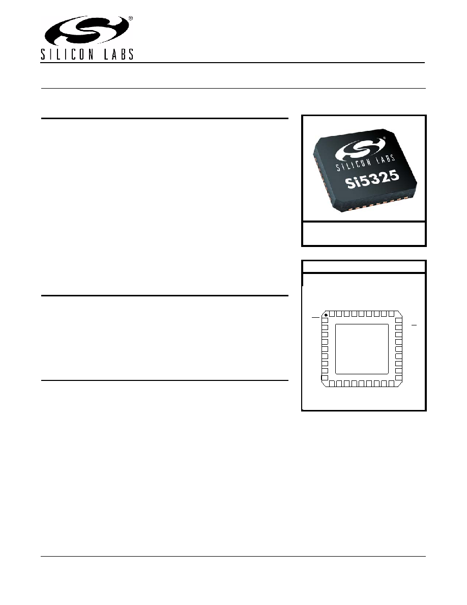
Small size: 6 x 6 mm 36-lead
QFN
Pb-free, ROHS compliant
SONET/SDH OC-48/STM-16 and
OC-192/STM-64
line cards
GbE/10GbE, 1/2/4/8/10GFC line
cards
ITU G.709 and custom FEC line
cards
Optical modules
Wireless basestations
Data converter clocking
xDSL
SONET/SDH + PDH clock synthesis
Test and measurement
Ordering Information:
See page 56.
Pin Assignments
1
2
3
29
30
31
32
33
34
35
36
20
21
22
23
24
25
26
27
10 11 12 13 14 15 16 17
4
5
6
7
8
NC
RST
C2B
INT_C1B
GND
VDD
GND
VD
D
VD
D
CL
K
IN2
+
CL
K
IN
2
–
NC
VD
D
CL
K
IN
1
+
CL
K
IN
1
–
CS_CA
SCL
SDA_SDO
A1
A2_SS
SDI
CL
K
O
UT1
–
NC
GN
D
VD
D
NC
CK
O
U
T
2
–
CK
O
U
T
2
+
CM
O
DE
GND
Pad
A0
GND
9
18
19
28
NC
GND
CL
K
O
U
T
1
+
相关PDF资料 |
PDF描述 |
|---|---|
| XC61CN2002MR-G | IC SUPERVISOR 2V SOT23-3 |
| M3AAK-1060K | IDC CABLE - MSC10K/MC10F/MSC10K |
| 1-6374659-0 | C/A LC TO LC MM 2.0MM 10M1 |
| H3DKH-5018M | IDC CABLE - HKR50H/AE50M/HPK50H |
| XR16V654DIV-0A-EB | EVAL BOARD FOR XR16V654D 64LQFP |
相关代理商/技术参数 |
参数描述 |
|---|---|
| Si5325A-B-GM | 功能描述:锁相环 - PLL uP-PROGRAMMABE CLK MULT 10 MHZ-1.4 GHZ RoHS:否 制造商:Silicon Labs 类型:PLL Clock Multiplier 电路数量:1 最大输入频率:710 MHz 最小输入频率:0.002 MHz 输出频率范围:0.002 MHz to 808 MHz 电源电压-最大:3.63 V 电源电压-最小:1.71 V 最大工作温度:+ 85 C 最小工作温度:- 40 C 封装 / 箱体:QFN-36 封装:Tray |
| SI5325A-B-GMR | 制造商:Silicon Laboratories Inc 功能描述: |
| Si5325A-C-GM | 功能描述:锁相环 - PLL uP-PROGRAMMABE CLK MULT 10 MHZ-1.4 GHZ RoHS:否 制造商:Silicon Labs 类型:PLL Clock Multiplier 电路数量:1 最大输入频率:710 MHz 最小输入频率:0.002 MHz 输出频率范围:0.002 MHz to 808 MHz 电源电压-最大:3.63 V 电源电压-最小:1.71 V 最大工作温度:+ 85 C 最小工作温度:- 40 C 封装 / 箱体:QFN-36 封装:Tray |
| SI5325A-C-GMR | 功能描述:时钟发生器及支持产品 mP-Program Precision Clk Multiplier 2/2 RoHS:否 制造商:Silicon Labs 类型:Clock Generators 最大输入频率:14.318 MHz 最大输出频率:166 MHz 输出端数量:16 占空比 - 最大:55 % 工作电源电压:3.3 V 工作电源电流:1 mA 最大工作温度:+ 85 C 安装风格:SMD/SMT 封装 / 箱体:QFN-56 |
| Si5325B-B-GM | 功能描述:锁相环 - PLL uP-PROGRAMMABE CLK MULT 10 MHZ-808 MHZ RoHS:否 制造商:Silicon Labs 类型:PLL Clock Multiplier 电路数量:1 最大输入频率:710 MHz 最小输入频率:0.002 MHz 输出频率范围:0.002 MHz to 808 MHz 电源电压-最大:3.63 V 电源电压-最小:1.71 V 最大工作温度:+ 85 C 最小工作温度:- 40 C 封装 / 箱体:QFN-36 封装:Tray |
发布紧急采购,3分钟左右您将得到回复。