- 您现在的位置:买卖IC网 > PDF目录98080 > SI5334B-A00124-GM (SILICON LABORATORIES) PLL BASED CLOCK DRIVER, QCC24 PDF资料下载
参数资料
| 型号: | SI5334B-A00124-GM |
| 厂商: | SILICON LABORATORIES |
| 元件分类: | 时钟及定时 |
| 英文描述: | PLL BASED CLOCK DRIVER, QCC24 |
| 封装: | 4 X 4 MM, ROHS COMPLIANT, MO-220VGGD-8, QFN-24 |
| 文件页数: | 11/34页 |
| 文件大小: | 233K |
| 代理商: | SI5334B-A00124-GM |
第1页第2页第3页第4页第5页第6页第7页第8页第9页第10页当前第11页第12页第13页第14页第15页第16页第17页第18页第19页第20页第21页第22页第23页第24页第25页第26页第27页第28页第29页第30页第31页第32页第33页第34页
Si5334
Preliminary Rev. 0.16
19
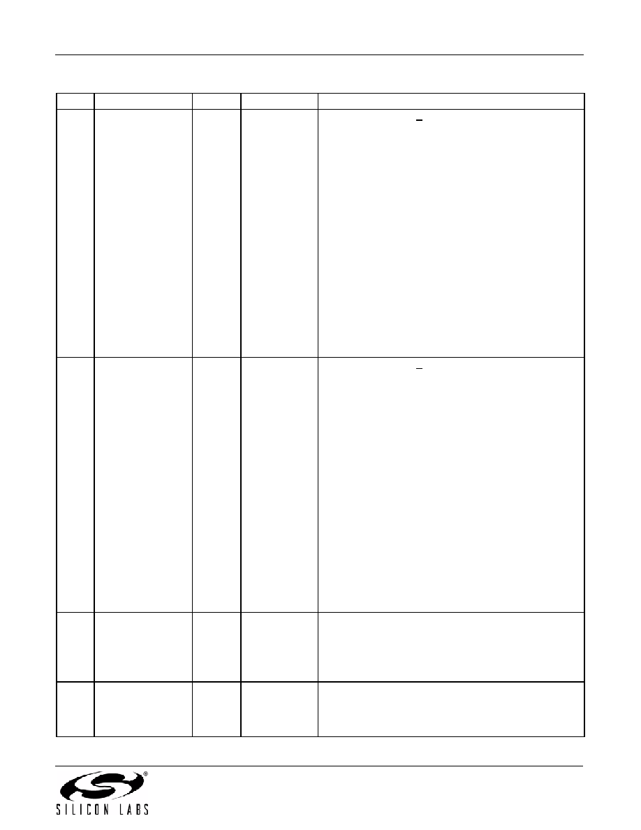
3IN3
I
Multi
Keep the input level > –0.1 V and < VDD+.1 V.
REFCLKSE
High impedance input for single-ended clock signals
such as CMOS. The input should be dc-coupled.
PINC
This pin function is active for devices Si5334D/E/F. A
positive pulse of greater than 100 ns width (followed by
>100 ns low) will increase the input to output device
latency by a factory-programmed amount. The function
of this pin is factory programmed.
FINC
This pin function is active for devices Si5334G/H/J. A
positive pulse of greater than 100 ns width (followed by
>100 ns low) will increase the output frequency of the
clock output by a factory-programmed amount. The
function of this pin is factory-programmed.
If this pin is unused, it should be grounded.
4IN4
I
LVCMOS
Keep the input level > –0.1 V and < VDD+ 0.1 V.
FDBKSE
High Impedance input for single-ended clock signals,
such as CMOS, when the zero delay mode of operation
is required. This input should be dc-coupled.
PDEC
This pin function is active for devices Si5334D/E/F. A
positive pulse of greater than 100 ns width (followed by
>100 ns low) will decrease the input to output device
latency by a factory-programmed amount. The function
of this pin is factory-programmed.
FDEC
This pin function is active for devices Si5334G/H/J. A
positive pulse of greater than 100 ns width (followed by
>100 ns low) will decrease the output frequency of the
clock output by a factory-programmed amount. The
function of this pin is factory-programmed.
If this pin is unused, it should be grounded.
5,6
IN5/IN6
I
Multi
FDBK/FDBKB
These pins form a differential input for feedback clock
signals when a zero delay mode of operation is in effect.
Always AC couple into these pins. When not is use
leave FDBK unconnected and connect FDBK to ground.
7
VDD
Supply
Core Supply Voltage
The device operates from a 1.8, 2.5, or 3.3 V supply. A
0.1 F bypass capacitor should be located very close to
this pin.
Table 15. Si5334 Pin Descriptions (Continued)
Pin #
Pin Name
I/O
Signal Type
Description
相关PDF资料 |
PDF描述 |
|---|---|
| SI5334C-A00099-GMR | PLL BASED CLOCK DRIVER, QCC24 |
| SI5334C-A00107-GM | PLL BASED CLOCK DRIVER, QCC24 |
| SI5334C-A00140-GMR | PLL BASED CLOCK DRIVER, QCC24 |
| SI5334B-A00109-GM | PLL BASED CLOCK DRIVER, QCC24 |
| SI5334B-A00121-GMR | PLL BASED CLOCK DRIVER, QCC24 |
相关代理商/技术参数 |
参数描述 |
|---|---|
| SI5334B-A00154-GM | 制造商:Silicon Laboratories Inc 功能描述:CLOCK - Rail/Tube |
| SI5334B-A00154-GMR | 制造商:Silicon Laboratories Inc 功能描述:CLOCK - Tape and Reel |
| SI5334B-A00156-GM | 制造商:Silicon Laboratories Inc 功能描述:CLOCK - Rail/Tube |
| SI5334B-A00156-GMR | 制造商:Silicon Laboratories Inc 功能描述:CLOCK - Tape and Reel |
| SI5334B-A00164-GM | 制造商:Silicon Laboratories Inc 功能描述:CLOCK - Rail/Tube |
发布紧急采购,3分钟左右您将得到回复。