- 您现在的位置:买卖IC网 > PDF目录2108 > SI5365-C-GQ (Silicon Laboratories Inc)IC CLOCK MULTIPLIER PROG 100TQFP PDF资料下载
参数资料
| 型号: | SI5365-C-GQ |
| 厂商: | Silicon Laboratories Inc |
| 文件页数: | 11/28页 |
| 文件大小: | 0K |
| 描述: | IC CLOCK MULTIPLIER PROG 100TQFP |
| 标准包装: | 90 |
| 系列: | DSPLL® |
| 类型: | 时钟乘法器 |
| PLL: | 是 |
| 输入: | 时钟 |
| 输出: | CML,CMOS,LVDS,LVPECL |
| 电路数: | 1 |
| 比率 - 输入:输出: | 4:5 |
| 差分 - 输入:输出: | 是/是 |
| 频率 - 最大: | 1.05GHz |
| 除法器/乘法器: | 无/是 |
| 电源电压: | 1.71 V ~ 2.75 V |
| 工作温度: | -40°C ~ 85°C |
| 安装类型: | 表面贴装 |
| 封装/外壳: | 100-TQFP |
| 供应商设备封装: | 100-TQFP(14x14) |
| 包装: | 托盘 |
第1页第2页第3页第4页第5页第6页第7页第8页第9页第10页当前第11页第12页第13页第14页第15页第16页第17页第18页第19页第20页第21页第22页第23页第24页第25页第26页第27页第28页
Si5365
Rev. 0.5
19
80
95
SFOUT1
SFOUT0
I
3-Level
Signal Format Select.
Three level inputs that select the output signal format (common mode
voltage and differential swing) for all of the clock outputs except
CKOUT5 (see DBL5).
Bypass mode is not available with CMOS outputs. When VDD = 3.3 V,
for thermal reasons, there are restrictions on the number of LVPECL
and CMOS outputs. See the Si53xx-RM reference manual for details.
These pins have both weak pullups and weak pulldowns and default to
M.
Some designs may require an external resistor voltage divider when
driven by an active device that will tri-state.
82
83
CKOUT1–
CKOUT1+
OMULTI
Clock Output 1.
Differential output clock with a frequency specified by FRQSEL and
FRQTBL. Output signal format is selected by SFOUT pins. Output is
differential for LVPECL, LVDS, and CML compatible modes. For CMOS
format, both output pins drive identical single-ended clock outputs.
85
DBL34
I
LVCMOS
Output 3 and 4 Disable.
Active high input. When active, entire CKOUT3 and CKOUT4 divider
and output buffer path is powered down. CKOUT3 and CKOUT4 out-
puts will be in tristate mode during powerdown.
This pin has a weak pullup.
87
88
CKOUT5–
CKOUT5+
OMULTI
Clock Output 5.
Fifth high-speed clock output with a frequency specified by FRQSEL
and FRQTBL. Output signal format is selected by SFOUT pins. Output
is differential for LVPECL, LVDS, and CML compatible modes. For
CMOS format, both output pins drive identical single-ended clock out-
puts.
92
93
CKOUT2+
CKOUT2–
OMULTI
Clock Output 2.
Differential output clock with a frequency specified by FRQSEL and
FRQTBL. Output signal format is selected by SFOUT pins. Output is
differential for LVPECL, LVDS, and CML compatible modes. For CMOS
format, both output pins drive identical single-ended clock outputs.
Table 6. Si5365 Pin Descriptions (Continued)
Pin #
Pin Name
I/O Signal Level
Description
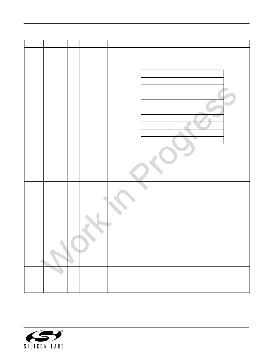
SFOUT[1:0]
Signal Format
HH
Reserved
HM
LVDS
HL
CML
MH
LVPECL
MM
Reserved
ML
LVDS—Low Swing
LH
CMOS
LM
Disable
LL
Reserved
相关PDF资料 |
PDF描述 |
|---|---|
| SI5366-C-GQ | IC CLOCK MULTIPLIER PREC 100TQFP |
| SI5367A-C-GQ | IC CLOCK MULTIPLIER PROG 100TQFP |
| SI5368A-C-GQ | IC CLK MULTIPLIER ATTEN 100TQFP |
| SI5369A-C-GQ | IC CLK MULT JITTER ATTEN 100TQFP |
| SI5374B-A-GL | IC CLK GEN/JITTER ATTEN 80LBGA |
相关代理商/技术参数 |
参数描述 |
|---|---|
| SI5365-C-GQR | 功能描述:时钟发生器及支持产品 Pin-Progrm Precision Clk Xplier 4In/5Out RoHS:否 制造商:Silicon Labs 类型:Clock Generators 最大输入频率:14.318 MHz 最大输出频率:166 MHz 输出端数量:16 占空比 - 最大:55 % 工作电源电压:3.3 V 工作电源电流:1 mA 最大工作温度:+ 85 C 安装风格:SMD/SMT 封装 / 箱体:QFN-56 |
| SI5365-EVB | 制造商:Silicon Laboratories Inc 功能描述: |
| SI5366 | 制造商:SILABS 制造商全称:SILABS 功能描述:PRECISION CLOCK MULTIPLIER/JITTER ATTENUATOR |
| Si5366-B-GQ | 功能描述:锁相环 - PLL PIN-PROGRAM CLK MULT /JITTER ATTEN 5 OUT RoHS:否 制造商:Silicon Labs 类型:PLL Clock Multiplier 电路数量:1 最大输入频率:710 MHz 最小输入频率:0.002 MHz 输出频率范围:0.002 MHz to 808 MHz 电源电压-最大:3.63 V 电源电压-最小:1.71 V 最大工作温度:+ 85 C 最小工作温度:- 40 C 封装 / 箱体:QFN-36 封装:Tray |
| SI5366-B-GQR | 制造商:Silicon Laboratories Inc 功能描述: |
发布紧急采购,3分钟左右您将得到回复。