- 您现在的位置:买卖IC网 > PDF目录8975 > SI5367C-C-GQR (Silicon Laboratories Inc)IC CLOCK MULTIPLIER PROG 100TQFP PDF资料下载
参数资料
| 型号: | SI5367C-C-GQR |
| 厂商: | Silicon Laboratories Inc |
| 文件页数: | 66/80页 |
| 文件大小: | 0K |
| 描述: | IC CLOCK MULTIPLIER PROG 100TQFP |
| 标准包装: | 250 |
| 系列: | DSPLL® |
| 类型: | 时钟乘法器 |
| PLL: | 是 |
| 输入: | 时钟 |
| 输出: | CML,CMOS,LVDS,LVPECL |
| 电路数: | 1 |
| 比率 - 输入:输出: | 4:5 |
| 差分 - 输入:输出: | 是/是 |
| 频率 - 最大: | 346MHz |
| 除法器/乘法器: | 无/是 |
| 电源电压: | 1.71 V ~ 2.75 V |
| 工作温度: | -40°C ~ 85°C |
| 安装类型: | 表面贴装 |
| 封装/外壳: | 100-TQFP |
| 供应商设备封装: | 100-TQFP(14x14) |
| 包装: | 带卷 (TR) |
第1页第2页第3页第4页第5页第6页第7页第8页第9页第10页第11页第12页第13页第14页第15页第16页第17页第18页第19页第20页第21页第22页第23页第24页第25页第26页第27页第28页第29页第30页第31页第32页第33页第34页第35页第36页第37页第38页第39页第40页第41页第42页第43页第44页第45页第46页第47页第48页第49页第50页第51页第52页第53页第54页第55页第56页第57页第58页第59页第60页第61页第62页第63页第64页第65页当前第66页第67页第68页第69页第70页第71页第72页第73页第74页第75页第76页第77页第78页第79页第80页
Si5367
Rev. 0.5
69
11
C3B
O
LVCMOS
CKIN3 Invalid Indicator.
This pin performs the CK3_BAD function if
CK3_BAD_PIN = 1 and is tristated if CK3_BAD_PIN =0.
Active polarity is controlled by CK_BAD_POL.
0 = No alarm on CKIN3.
1 = Alarm on CKIN3.
12
INT_ALM
O
LVCMOS
Interrupt/Alarm Output Indicator.
This pin functions as a maskable interrupt output with
active polarity controlled by the INT_POL register bit.
The INT output function can be turned off by setting
INT_PIN = 0. If the ALRMOUT function is desired
instead on this pin, set ALRMOUT_PIN = 1 and
INT_PIN =0.
0 = ALRMOUT not active.
1 = ALRMOUT active.
The active polarity is controlled by CK_BAD_POL. If no
function is selected, the pin tristates.
13
57
CS0_C3A
CS1_C4A
I/O
LVCMOS
Input Clock Select/CKIN3 or CKIN4 Active Clock
Indicator.
Input: If manual clock selection is chosen, and if
CKSEL_PIN = 1, the CKSEL pins control clock
selection and the CKSEL_REG bits are ignored.
If configured as inputs, these pins must not
float.
Output: If CKSEL_PIN =0, the CKSEL_REG register
bits control this function.
If auto clock selection is enabled, then they
serve as the CKIN_n active clock indicator.
0 = CKIN3 (CKIN4) is not the active input clock
1 = CKIN3 (CKIN4) is currently the active input
to the PLL
The CKn_ACTV_REG bit always reflects the
active clock status for CKIN_n. If
CKn_ACTV_PIN = 1, this status will also be
reflected on the CnA pin with active polarity con-
trolled by the CK_ACTV_POL bit. If
CKn_ACTV_PIN = 0, this output tristates.
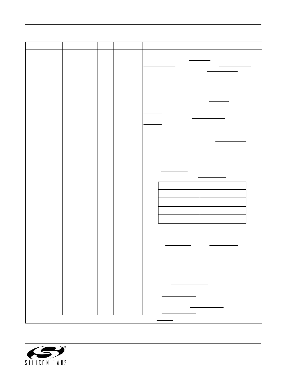
Table 11. Si5367 Pin Descriptions (Continued)
Pin #
Pin Name
I/O
Signal Level
Description
Note: Internal register names are indicated by underlined italics, e.g. INT_PIN. See Si5368 Register Map.
CS[1:0]
Active Input Clock
00
CKIN1
01
CKIN2
10
CKIN3
11
CKIN4
相关PDF资料 |
PDF描述 |
|---|---|
| VE-2NB-MW-F2 | CONVERTER MOD DC/DC 95V 100W |
| VI-B0X-MY-F4 | CONVERTER MOD DC/DC 5.2V 50W |
| VI-BTV-MY-F1 | CONVERTER MOD DC/DC 5.8V 50W |
| VE-J4D-MZ-F3 | CONVERTER MOD DC/DC 85V 25W |
| VE-B4Z-MU-F2 | CONVERTER MOD DC/DC 2V 80W |
相关代理商/技术参数 |
参数描述 |
|---|---|
| SI5367-EVB | 制造商:Silicon Laboratories Inc 功能描述: |
| SI5368 | 制造商:SILABS 制造商全称:SILABS 功能描述:ANY-RATE PRECISION CLOCK MULTIPLIER/JITTER ATTENUATOR |
| Si5368A-B-GQ | 功能描述:锁相环 - PLL ANY-RATE CLK MULT JITTER ATTEN 5 OUTS RoHS:否 制造商:Silicon Labs 类型:PLL Clock Multiplier 电路数量:1 最大输入频率:710 MHz 最小输入频率:0.002 MHz 输出频率范围:0.002 MHz to 808 MHz 电源电压-最大:3.63 V 电源电压-最小:1.71 V 最大工作温度:+ 85 C 最小工作温度:- 40 C 封装 / 箱体:QFN-36 封装:Tray |
| SI5368A-B-GQR | 制造商:Silicon Laboratories Inc 功能描述: |
| Si5368A-C-GQ | 功能描述:锁相环 - PLL ANY-RATE CLK MULT JITTER ATTEN 5 OUTS RoHS:否 制造商:Silicon Labs 类型:PLL Clock Multiplier 电路数量:1 最大输入频率:710 MHz 最小输入频率:0.002 MHz 输出频率范围:0.002 MHz to 808 MHz 电源电压-最大:3.63 V 电源电压-最小:1.71 V 最大工作温度:+ 85 C 最小工作温度:- 40 C 封装 / 箱体:QFN-36 封装:Tray |
发布紧急采购,3分钟左右您将得到回复。