- 您现在的位置:买卖IC网 > PDF目录17135 > SI85XX20AQFN-KIT (Silicon Laboratories Inc)KIT DEVELOPMENT FOR SI85XX20AQFN PDF资料下载
参数资料
| 型号: | SI85XX20AQFN-KIT |
| 厂商: | Silicon Laboratories Inc |
| 文件页数: | 13/36页 |
| 文件大小: | 0K |
| 描述: | KIT DEVELOPMENT FOR SI85XX20AQFN |
| 标准包装: | 1 |
| 传感器类型: | 电流传感器 |
| 传感范围: | 20A |
| 接口: | 模拟 |
| 电源电压: | 5V |
| 嵌入式: | 否 |
| 已供物品: | 板 |
| 已用 IC / 零件: | Si5313 |
第1页第2页第3页第4页第5页第6页第7页第8页第9页第10页第11页第12页当前第13页第14页第15页第16页第17页第18页第19页第20页第21页第22页第23页第24页第25页第26页第27页第28页第29页第30页第31页第32页第33页第34页第35页第36页
�� �
�
�Si85xx�
�3.� Application� Information�
�Ground�
�Ground�
�3.1.� Board� Layout�
�Plane� Edge�
�Top� View�
�Plane� Edge�
�The� Si85xx� is� connected� in� the� series� path� of� the� current�
�to� be� measured.� The� Si85xx� must� be� located� as� far� as�
�possible� from� transformer� and� other� magnetic� field�
�sources.� Like� other� analog� components,� the� Si85xx�
�should� be� powered� from� a� low-noise� dc� source� and,�
�preferably,� to� a� low-noise� analog� ground� plane.�
�Recommended� bypass� capacitors� are� 1� μF� in� parallel�
�with� a� 0.1� μF,� positioned� as� close� to� the� Si85xx� as�
�VDD� Pin�
�Mode� Pin�
�(Non-Ping-Pong)�
�VDD� Fly� Wire�
�Current�
�Carrying� Slug�
�possible.� When� using� the� Si850x� (single� output�
�versions),� all� three� ground� pins� MUST� be� connected� to�
�the� same� ground� point,� and� both� VDD1� and� VDD2� pins�
�MUST� be� tied� to� the� VDD� system� power� supply.�
�3.2.� Layout� Requirements�
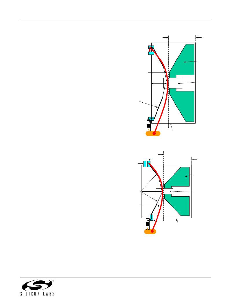
�The� Si85xx� requires� special� layout� techniques� to� ensure�
�proper� operation� (see� Figures� 9� and� 10).� Due� to� the�
�close� proximity� of� the� current-carrying� slug� and� current�
�sensor� silicon,� magnetic� coupling� between� the� current-�
�carrying� slug� and� the� silicon� can� form� a� ground� loop�
�causing� the� output� voltage� to� be� 0� V� even� though�
�current� is� flowing� through� the� slug.� To� eliminate� any�
�Bonding� Wire�
�Gnd� Pin�
�Bypass� Capacitor�
�5� V� VDD� Trace�
�3.5� mm�
�SOIC� Package�
�Current�
�Sensor� Die�
�such� coupling� issues,� a� red� fly-wire� VDD� trace� (see�
�Figures� 9� and� 10)� should� be� implemented� in� the� layout.�
�For� the� SOIC� package,� the� red� fly-wire� trace� should� be�
�Figure� 9.� SOIC� Layout� Requirements�
�approximately� 3.5� mm� from� the� center� edge� of� the�
�package� intersecting� approximately� in� the� center� of� the�
�package� (see� Figure� 9).� For� the� QFN� package,� the� red�
�fly-wire� should� be� approximately� in� the� center� of� the�
�package� (see� Figure� 10).� Standard� wire� thicknesses� for�
�10� mA� current-carrying� capabilities� should� be� used.�
�Moreover,� note� that� the� fly-wire� trace� should� be�
�completely� under� the� ground� plane� since� this� will� also�
�Ground� Plane� Edge�
�VDD� Pin�
�Mode� Pin�
�(Non-Ping-Pong)�
�Top� View�
�Ground�
�Plane� Edge�
�Current�
�Carrying� Slug�
�reduce� coupling.�
�Regarding� isolation� voltage� requirements,� the� trace�
�Bonding�
�Wires�
�2� mm�
�Current�
�Sensor� Die�
�does� not� need� to� follow� the� lead� frame� and� bonding�
�traces� exactly,� as� long� as� the� net� magnetic� flux� is� close�
�to� zero.� The� goal� here� is� to� keep� the� magnetic� coupling�
�small� and,� at� the� same� time,� keep� the� isolation� distance�
�large.� Moreover,� to� ensure� that� the� layout� meets� the�
�VDD�
�Fly� Wire�
�design’s� required� creepage� and� clearance�
�Bypass� Capacitor�
�Gnd� Pin�
�QFN� Package�
�requirements,� the� VDD� trace� should� be� placed� on� one�
�of� the� inner� layers� or� even� the� back� side� of� the� board.�
�For� example,� one� can� lay� out� the� return� VDD� trace� on�
�the� other� side� of� the� PCB� so� the� PCB� itself� can� help� to�
�provide� high� isolation� voltage.�
�5V� VDD� Trace�
�Figure� 10.� QFN� Layout� Requirements�
�Preliminary� Rev.� 0.4�
�13�
�相关PDF资料 |
PDF描述 |
|---|---|
| PCV1J330MCL1GS | CAP ALUM 33UF 63V 20% SMD |
| NC-254097-10-9 | LABEL NYLON CLOTH 25.4X0.97MM |
| ECC06DRYH-S734 | CONN EDGECARD 12POS DIP .100 SLD |
| SI85XX5KV-EVB | EVAL BOARD FOR SI85XX5KV |
| HBC08DREI-S13 | CONN EDGECARD 16POS .100 EXTEND |
相关代理商/技术参数 |
参数描述 |
|---|---|
| Si85XX5KV-EVB | 功能描述:电流传感器开发工具 5kV Current Sensor Eval Board RoHS:否 制造商:Texas Instruments 工具用于评估:LMP91000 接口类型:USB 工作电压:2.7 V to 5.25 V 最大工作温度: |
| Si85XX-EVB | 功能描述:电流传感器开发工具 10A Current Sensor Eval Board RoHS:否 制造商:Texas Instruments 工具用于评估:LMP91000 接口类型:USB 工作电压:2.7 V to 5.25 V 最大工作温度: |
| SI8600AB-B-IS | 制造商:Silicon Laboratories Inc 功能描述:2.5 KV BIDIRECTIONAL I2C ISOLATOR, 1.7MHZ, SOIC8, LEAD FREE, - Rail/Tube |
| SI8600AB-B-ISR | 制造商:Silicon Laboratories Inc 功能描述:2.5 KV BIDIRECTIONAL I2C ISOLATOR, 1.7MHZ, SOIC8, LEAD FREE, - Tape and Reel |
| Si8600AC-B-IS | 功能描述:隔离器接口集成电路 3.75kV Bidirect I2C Isolator 1.7MHz ADuM RoHS:否 制造商:Texas Instruments 通道数量:2 传播延迟时间: 电源电压-最大:5.5 V 电源电压-最小:3 V 电源电流:3.6 mA 功率耗散: 最大工作温度:+ 125 C 安装风格: 封装 / 箱体:SOIC-8 封装:Tube |
发布紧急采购,3分钟左右您将得到回复。