- 您现在的位置:买卖IC网 > PDF目录67969 > SJ80C52XXX-12SC (ATMEL CORP) 8-BIT, MROM, 12 MHz, MICROCONTROLLER, CQCC44 PDF资料下载
参数资料
| 型号: | SJ80C52XXX-12SC |
| 厂商: | ATMEL CORP |
| 元件分类: | 微控制器/微处理器 |
| 英文描述: | 8-BIT, MROM, 12 MHz, MICROCONTROLLER, CQCC44 |
| 封装: | JLCC-44 |
| 文件页数: | 10/20页 |
| 文件大小: | 194K |
| 代理商: | SJ80C52XXX-12SC |
6
42073AS-MCU Wireless-02/13
ATmega2564/1284/644RFR2
source current if the pull-up resistors are activated. The Port E pins are tri-stated when
a reset condition becomes active, even if the clock is not running.
Due to the low pin count of the QFN48 package port E6 is not connected to a pin.
Port
E
also
provides
functions
of
various
special
features
of
the
ATmega2564/1284/644RFR2.
3.2.10 Port F (PF7..PF5,PF4/3,PF2...PF0)
Internally Port F is an 8-bit bi-directional I/O port with internal pull-up resistors (selected
for each bit). The Port F output buffers have symmetrical drive characteristics with both
high sink and source capability. As inputs, Port F pins that are externally pulled low will
source current if the pull-up resistors are activated. The Port F pins are tri-stated when
a reset condition becomes active, even if the clock is not running.
Due to the low pin count of the QFN48 package port F3 and F4 are connected to the
same pin. The I/O configuration should be done carefully in order to avoid excessive
power dissipation.
Port
F
also
provides
functions
of
various
special
features
of
the
ATmega2564/1284/644RFR2.
3.2.11 Port G (PG4,PG3,PG1)
Internally Port G is a 6-bit bi-directional I/O port with internal pull-up resistors (selected
for each bit). The Port G output buffers have symmetrical drive characteristics with both
high sink and source capability. However the driver strength of PG3 and PG4 is
reduced compared to the other port pins. The output voltage drop (VOH, VOL) is higher
while the leakage current is smaller. As inputs, Port G pins that are externally pulled low
will source current if the pull-up resistors are activated. The Port G pins are tri-stated
when a reset condition becomes active, even if the clock is not running.
Due to the low pin count of the QFN48 package port G0, G2 and G5 are not connected
to a pin.
Port
G
also
provides
functions
of
various
special
features
of
the
ATmega2564/1284/644RFR2.
3.2.12 AVSS_RFP
AVSS_RFP is a dedicated ground pin for the bi-directional, differential RF I/O port.
3.2.13 AVSS_RFN
AVSS_RFN is a dedicated ground pin for the bi-directional, differential RF I/O port.
3.2.14 RFP
RFP is the positive terminal for the bi-directional, differential RF I/O port.
3.2.15 RFN
RFN is the negative terminal for the bi-directional, differential RF I/O port.
3.2.16 RSTN
Reset input. A low level on this pin for longer than the minimum pulse length will
generate a reset, even if the clock is not running. Shorter pulses are not guaranteed to
generate a reset.
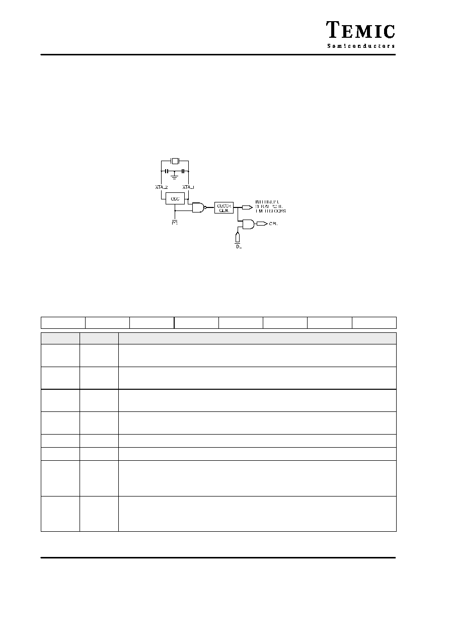
3.2.17 XTAL1
Input to the inverting 16MHz crystal oscillator amplifier. In general a crystal between
XTAL1 and XTAL2 provides the 16MHz reference clock of the radio transceiver.
3.2.18 XTAL2
Output of the inverting 16MHz crystal oscillator amplifier.
相关PDF资料 |
PDF描述 |
|---|---|
| SD80C52XXX-12SV | 8-BIT, MROM, 12 MHz, MICROCONTROLLER, CDIP40 |
| SC80C32XXX-12SB | 8-BIT, 12 MHz, MICROCONTROLLER, CDIP40 |
| SC80C32XXX-36SC | 8-BIT, 36 MHz, MICROCONTROLLER, CDIP40 |
| SD80C52XXX-36 | 8-BIT, MROM, 36 MHz, MICROCONTROLLER, CDIP40 |
| SD80C52XXX-36/883 | 8-BIT, MROM, 36 MHz, MICROCONTROLLER, CDIP40 |
相关代理商/技术参数 |
参数描述 |
|---|---|
| SJ81200 | 制造商:Rochester Electronics LLC 功能描述:- Bulk |
| SJ83100 | 制造商:ON Semiconductor 功能描述:SJ83100 - Trays 制造商:Rochester Electronics LLC 功能描述:- Bulk |
| SJ83180 | 制造商:ON Semiconductor 功能描述:NPN TO-3 METAL PWR TRANSISTOR - Trays 制造商:Rochester Electronics LLC 功能描述:NPN TO-3 METAL PWR TRANSISTOR - Bulk |
| SJ84140 | 制造商:Rochester Electronics LLC 功能描述:- Bulk |
| SJ-870 | 制造商:NEL 制造商全称:Nel Frequency Controls,inc 功能描述:CRYSTAL CLOCK OSCILLATORS |
发布紧急采购,3分钟左右您将得到回复。