- 您现在的位置:买卖IC网 > PDF目录225191 > SL1461SA/KG/MPAD (INTEL CORP) SPECIALTY TELECOM CIRCUIT, PDSO16 PDF资料下载
参数资料
| 型号: | SL1461SA/KG/MPAD |
| 厂商: | INTEL CORP |
| 元件分类: | 通信及网络 |
| 英文描述: | SPECIALTY TELECOM CIRCUIT, PDSO16 |
| 封装: | 0.150 INCH, MS-012AC, SOIC-16 |
| 文件页数: | 9/13页 |
| 文件大小: | 377K |
| 代理商: | SL1461SA/KG/MPAD |
5
SL1461SA
Advance Information
DESIGN OF PLL LOOP PARAMETERS
Fig.4
VCO
R2
C1
BASEBAND OUTPUT
R1
RF INPUT
GAIN = K0 RAD SEC/VOLT
GAIN = KD VOLT/RAD
The SL1461SA is normally used as a type 1 second order
loop and can be represented by the above diagram. For such
a system the following parameters apply;
1
2
1
K
0KD
2
n
2
n
and
where:
K0 is the VCO gain in radian seconds per volt
KD is the phase detector gain in volts per radian
n is the natural loop bandwidth
is the loop damping factor
R1 is loop amplifier input impedance
Note:
K0 is dependant on sensitivity of VCO used.
KD = 0.25V/rad single ended, 0.5V/rad differential
From these factors the loop 3dB bandwidth can be determined
from the following expression;
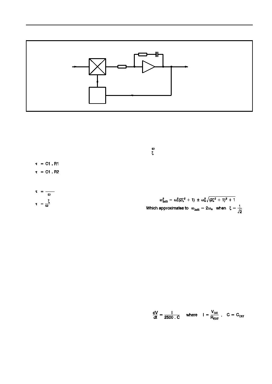
AFC FACILITY
The SL1461SA contains an analog frequency error
detect circuit, which generates DC voltage proportional to the
integral of frequency error. If the incident RF is high then the
AFC voltage increases, if low then the voltage decreases. The
AFC voltage can then be converted by an ADC to be read by
the micro controller for frequency fine tuning; if used in an I2C
system it is recommended the device is used with either the
SP5055 or SP5056 frequency synthesiser which contains an
internal ADC readable via the I2C bus.
The voltage corresponding to frequency alignment is
arbitrary and user defined; if used with the SP5055 it is
suggested the aligned voltage is 0.375 VCC , corresponding to
the centre code of the ADC on port 6.
The AFC detect circuit contains a deadband centre
around the aligned frequency. The deadband can be adjusted
from zero window to approximately 25MHz width assuming an
oscillator dF/dV of 15MHz/V. If the incident RF is within this
window the AFC voltage does not integrate, except by
component leakage.
With reference to Fig.5; in normal operation the
demodulated video is fed to a dual comparator where it is
compared with two reference voltages, corresponding to the
extremes of the deadband, or window. These voltages are
variable and set by the window adjust input.
The comparators produce two digital outputs
corresponding to voltages above or below the voltage
window, or frequency above or below deadband. These digital
control signals are used to control a complimentary current
source pump. The current signals are then fed to the input of
an amplifier which is arranged as an integrator, so integrating
the
pulses into a DC voltage.
If the frequency is correctly aligned both the current
source and sink are disabled, therefore the DC output voltage
remains constant. There will be a small drift due to component
leakage; the maximum drift can be calculated from;
相关PDF资料 |
PDF描述 |
|---|---|
| SL1461SA/KG/MPAS | SPECIALTY TELECOM CIRCUIT, PDSO16 |
| SL1461SA/KG/MPBD | SPECIALTY TELECOM CIRCUIT, PDSO16 |
| SL1461SA/KG/MPBS | SPECIALTY TELECOM CIRCUIT, PDSO16 |
| SL1K-67132L-55SHXXX | 2K X 8 MULTI-PORT SRAM, 55 ns, CDIP48 |
| SL1K-67142V-55SHXXX | 2K X 8 MULTI-PORT SRAM, 55 ns, CDIP48 |
相关代理商/技术参数 |
参数描述 |
|---|---|
| SL1466 | 制造商:ZARLINK 制造商全称:Zarlink Semiconductor Inc 功能描述:Wideband PLL FM Demodulator |
| SL1466KG | 制造商:ZARLINK 制造商全称:Zarlink Semiconductor Inc 功能描述:Wideband PLL FM Demodulator |
| SL1466QP1S | 制造商:ZARLINK 制造商全称:Zarlink Semiconductor Inc 功能描述:Wideband PLL FM Demodulator |
| SL1496C | 制造商:PLW 功能描述:1496C 制造商:PSSB 功能描述:1496C |
| SL14B | 制造商:SR COMPONENTS 功能描述: 制造商:SR Components Inc 功能描述: |
发布紧急采购,3分钟左右您将得到回复。