- 您现在的位置:买卖IC网 > PDF目录9059 > SL15300ZC (Silicon Laboratories Inc)IC CLOCK SSCG 1PLL 2CH 8TSSOP PDF资料下载
参数资料
| 型号: | SL15300ZC |
| 厂商: | Silicon Laboratories Inc |
| 文件页数: | 5/16页 |
| 文件大小: | 0K |
| 描述: | IC CLOCK SSCG 1PLL 2CH 8TSSOP |
| 标准包装: | 100 |
| 系列: | * |
Rev 2.0, October 11, 2010
Page 13 of 16
SL15300
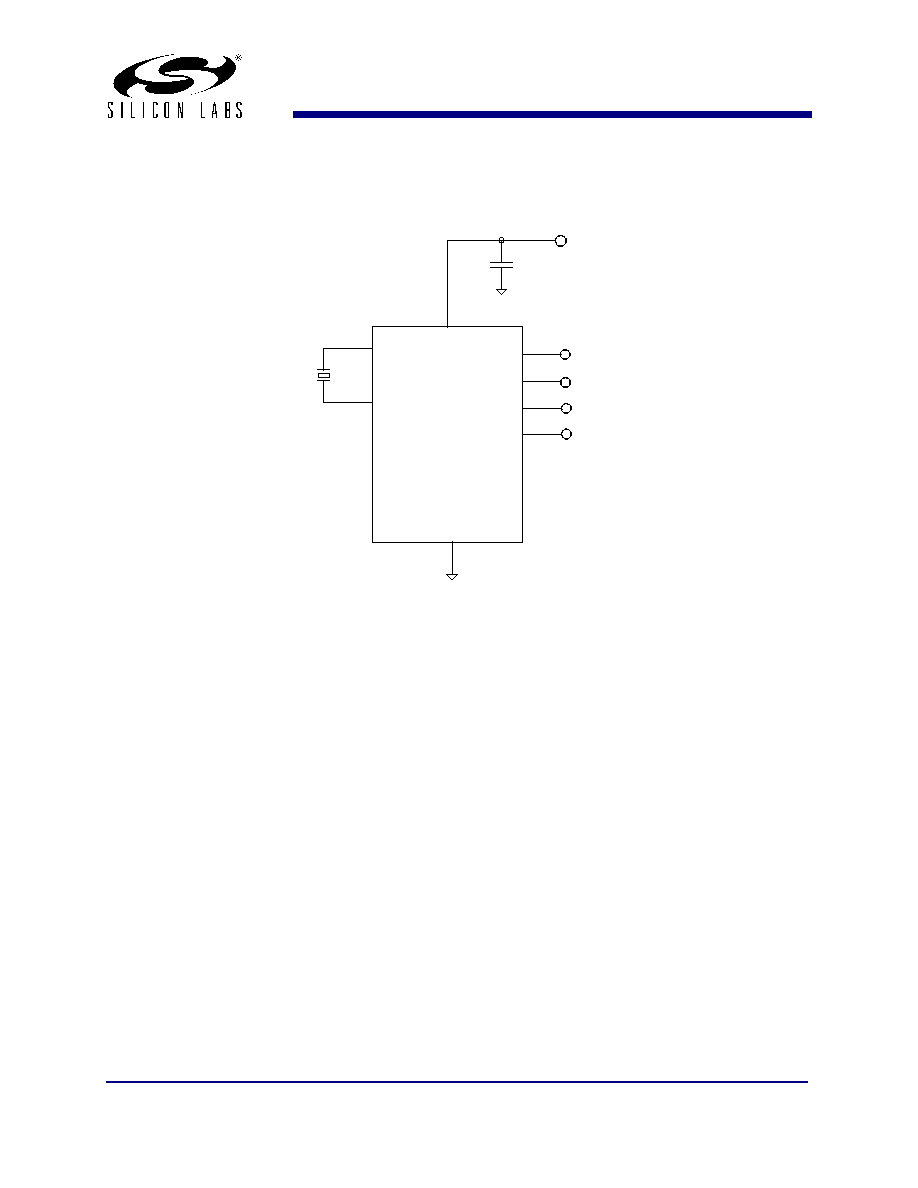
External Components & Design Considerations
Typical Application Schematic
SL15300
XIN(3)
VDD(1)
XOUT(2)
SSCLK1(7)
SSCLK3(4)
66 MHz, +/-1.5% Spread
27MHz
0.1
μF
VSS(5)
SSCLK2(8)
27 MHz, No Spread
VDD
REFCLK(6)
66 MHz, +/-1.5% Spread
33 MHz, +/-1.5% Spread
Comments and Recommendations
Decoupling Capacitor:
A decoupling capacitor of 0.1μF must be used between VDD and VSS on the pins 1 and 5.
Place the capacitor on the component side of the PCB as close to the VDD pin as possible. The PCB trace to the
VDD pin and to the GND via should be kept as short as possible Do not use vias between the decoupling capacitor
and the VDD pin.
Series Termination Resistor: A series termination resistor is recommended if the distance between the outputs
(SSCLK or REFCLK pins) and the load is over 1 inch. The nominal impedance of the SSCLK outpu
t is about 30 Ω.
Use 20 Ω resistor in series with the output to terminate 50Ω trace impedance and place 20 Ω resistor as close to the
SSCLK output as possible.
Crystal and Crystal Load: Use only parallel resonant fundamental crystals. DO NOT USE higher overtone crystals.
To meet the crystal initial accuracy specification (in ppm); the internal on-chip programmable capacitors PCin and
PCout must be programmed to match the crystal load requirement. These values are given by the formula below:
PCin(pF) =PCout(pF)= [(CL(pF) – Cp(pF)/2)] x 2
Where CL is crystal load capacitor as given by the crystal datasheet and Cp(pF) is the compensation factor for the
total parasitic capacitance at XIN or XOUT pin including PCB related parasitic capacitance.
As an example; if a crystal with CL=18pF is used and Cp=4pF, by using the above formula, PCin=PCout=[(18-(4/2)] x
2 = 32pF. Programming PCin and PCout to 32pF assures that this crystal sees an equivalent load of 18pF and no
other external crystal load capacitor is needed. Deviating from the crystal load specification could cause an increase
in frequency accuracy in ppm. Refer to the Table 5 for the recommended crystal specifications.
相关PDF资料 |
PDF描述 |
|---|---|
| VE-J1J-MZ-F2 | CONVERTER MOD DC/DC 36V 25W |
| VE-J1J-MZ-F1 | CONVERTER MOD DC/DC 36V 25W |
| SL15100ZC | IC CLOCK SSCG 1PLL 2CH 8TSSOP |
| 74LVX138SJ | DECODER/DEMUX 1-OF-8 LV 16SOP |
| ICS487G-25LFT | IC QUAD PLL FOR DTV 16-TSSOP |
相关代理商/技术参数 |
参数描述 |
|---|---|
| SL15300ZCT | 功能描述:时钟发生器及支持产品 1-200MHz 1PLL 2 Out CG/SSCG 3.3-2.5V RoHS:否 制造商:Silicon Labs 类型:Clock Generators 最大输入频率:14.318 MHz 最大输出频率:166 MHz 输出端数量:16 占空比 - 最大:55 % 工作电源电压:3.3 V 工作电源电流:1 mA 最大工作温度:+ 85 C 安装风格:SMD/SMT 封装 / 箱体:QFN-56 |
| SL15300ZC-XXX | 制造商:SPECTRALINEAR 制造商全称:SPECTRALINEAR 功能描述:Programmable Spread Spectrum Clock Generator (SSCG) |
| SL15300ZC-XXXT | 制造商:SPECTRALINEAR 制造商全称:SPECTRALINEAR 功能描述:Programmable Spread Spectrum Clock Generator (SSCG) |
| SL15300ZI | 功能描述:时钟发生器及支持产品 1-200MHz 1PLL 2 Out CG/SSCG 3.3-2.5V RoHS:否 制造商:Silicon Labs 类型:Clock Generators 最大输入频率:14.318 MHz 最大输出频率:166 MHz 输出端数量:16 占空比 - 最大:55 % 工作电源电压:3.3 V 工作电源电流:1 mA 最大工作温度:+ 85 C 安装风格:SMD/SMT 封装 / 箱体:QFN-56 |
| SL15300ZIT | 功能描述:时钟发生器及支持产品 1-200MHz 1PLL 2 Out CG/SSCG 3.3-2.5V RoHS:否 制造商:Silicon Labs 类型:Clock Generators 最大输入频率:14.318 MHz 最大输出频率:166 MHz 输出端数量:16 占空比 - 最大:55 % 工作电源电压:3.3 V 工作电源电流:1 mA 最大工作温度:+ 85 C 安装风格:SMD/SMT 封装 / 箱体:QFN-56 |
发布紧急采购,3分钟左右您将得到回复。