- 您现在的位置:买卖IC网 > PDF目录98081 > SL2309ZC-1 2309 SERIES, PLL BASED CLOCK DRIVER, 4 TRUE OUTPUT(S), 0 INVERTED OUTPUT(S), PDSO16 PDF资料下载
参数资料
| 型号: | SL2309ZC-1 |
| 元件分类: | 时钟及定时 |
| 英文描述: | 2309 SERIES, PLL BASED CLOCK DRIVER, 4 TRUE OUTPUT(S), 0 INVERTED OUTPUT(S), PDSO16 |
| 封装: | 4.40 MM, ROHS COMPLIANT, TSSOP-16 |
| 文件页数: | 1/12页 |
| 文件大小: | 248K |
| 代理商: | SL2309ZC-1 |
Rev 1.1, May 29, 2007
Page 1 of 12
2200 Laurelwood Road, Santa Clara, CA 95054 Tel: (408) 855-0555 Fax: (408) 855-0550 www.SpectraLinear.com
SL2309
Low Jitter and Skew 10 to 140 MHz Zero Delay Buffer (ZDB)
Key Features
10 to 140 MHz operating frequency range
Low output clock skew: 50ps-typ
Low output clock jitter:
50 ps-typ cycle-to-cycle jitter
Low part-to-part output skew: 150 ps-typ
3.3 V power supply range
Low power dissipation:
28 mA-max at 66 MHz
44 mA –max at 140 MHz
One input drives 9 outputs organized as 4+4+1
Select mode to bypass PLL or tri-state outputs
SpreadThru PLL that allows use of SSCG
Standard and High-Drive options
Available in 16-pin SOIC and TSSOP packages
Available in Commercial and Industrial grades
Applications
Printers and MFPs
Digital Copiers
PCs and Work Stations
DTV
Routers, Switchers and Servers
Digital Embeded Systems
Description
The SL2309 is a low skew, low jitter and low power Zero
Delay Buffer (ZDB) designed to produce up to nine (9)
clock outputs from one (1) reference input clock, for high
speed clock distribution applications.
The product has an on-chip PLL which locks to the input
clock at CLKIN and receives its feedback internally from
the CLKOUT pin.
The SL2309 has two (2) clock driver banks each with four
(4) clock outputs. These outputs are controlled by two (2)
select input pins S1 and S2. When only four (4) outputs
are needed, four (4) bank-B output clock buffers can be tri-
stated to reduce power dissipation and jitter. The select
inputs can also be used to tri-state both banks A and B or
drive them directly from the input bypassing the PLL and
making the product behave like a Non-Zero Delay Buffer
(NZDB).
The high-drive (-1H) version operates up to 140MHz and
low drive (-1) version operates up to 100MHz at 3.3V.
Benefits
Up to nine (9) distribution of input clock
Standard and High-Dirive levels to control impedance
level, frequency range and EMI
Low power dissipation, jitter and skew
Low cost
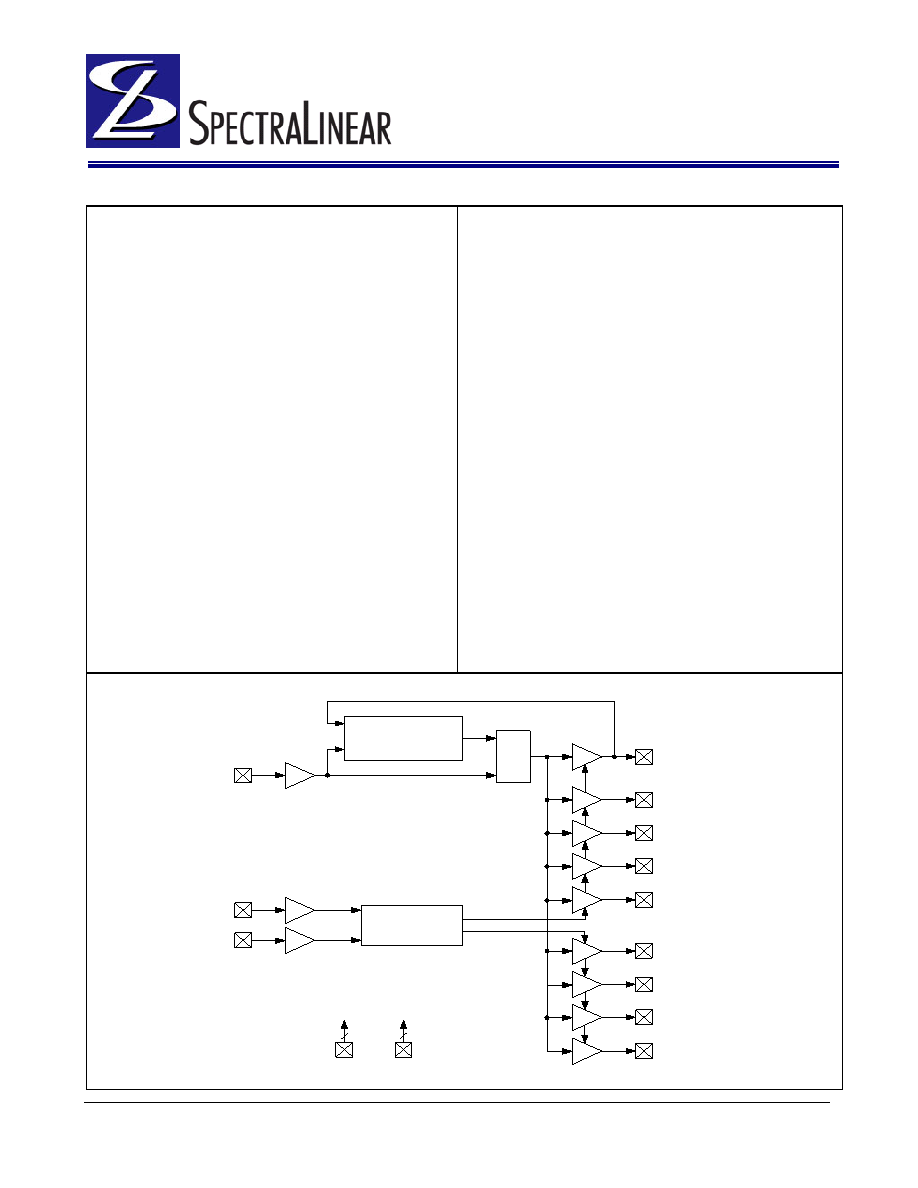
Block Diagram
Low Pow er and
Low Jitter
PLL
MU X
Input Selection
D ecoding Logic
VD D
GN D
2
S2
S1
CLK IN
C LKO UT
CLK A1
CLK A2
C LKA3
CLKA4
CLKB1
C LKB2
C LKB3
C LKB4
相关PDF资料 |
PDF描述 |
|---|---|
| SL23EP04NZZC-1ZT | 23EP SERIES, LOW SKEW CLOCK DRIVER, 4 TRUE OUTPUT(S), 0 INVERTED OUTPUT(S), PDSO8 |
| SL23EP04NZZC-1Z | 23EP SERIES, LOW SKEW CLOCK DRIVER, 4 TRUE OUTPUT(S), 0 INVERTED OUTPUT(S), PDSO8 |
| SL23EP04NZZI-1Z | 23EP SERIES, LOW SKEW CLOCK DRIVER, 4 TRUE OUTPUT(S), 0 INVERTED OUTPUT(S), PDSO8 |
| SL23EP04NZZI-1T | 23EP SERIES, LOW SKEW CLOCK DRIVER, 4 TRUE OUTPUT(S), 0 INVERTED OUTPUT(S), PDSO8 |
| SL23EP04NZZI-1ZT | 23EP SERIES, LOW SKEW CLOCK DRIVER, 4 TRUE OUTPUT(S), 0 INVERTED OUTPUT(S), PDSO8 |
相关代理商/技术参数 |
参数描述 |
|---|---|
| SL2309ZC-1H | 功能描述:时钟缓冲器 10-140MHz 9 Outputs ZDB 3.3V High Drive RoHS:否 制造商:Texas Instruments 输出端数量:5 最大输入频率:40 MHz 传播延迟(最大值): 电源电压-最大:3.45 V 电源电压-最小:2.375 V 最大功率耗散: 最大工作温度:+ 85 C 最小工作温度:- 40 C 封装 / 箱体:LLP-24 封装:Reel |
| SL2309ZC-1HT | 功能描述:时钟缓冲器 10-140MHz 9 Outputs ZDB 3.3V High Drive RoHS:否 制造商:Texas Instruments 输出端数量:5 最大输入频率:40 MHz 传播延迟(最大值): 电源电压-最大:3.45 V 电源电压-最小:2.375 V 最大功率耗散: 最大工作温度:+ 85 C 最小工作温度:- 40 C 封装 / 箱体:LLP-24 封装:Reel |
| SL2309ZC-1T | 功能描述:时钟缓冲器 10-140MHz 9 Outputs ZDB 3.3V RoHS:否 制造商:Texas Instruments 输出端数量:5 最大输入频率:40 MHz 传播延迟(最大值): 电源电压-最大:3.45 V 电源电压-最小:2.375 V 最大功率耗散: 最大工作温度:+ 85 C 最小工作温度:- 40 C 封装 / 箱体:LLP-24 封装:Reel |
| SL2309ZI-1 | 功能描述:时钟缓冲器 10-140MHz 9 Outputs ZDB 3.3V RoHS:否 制造商:Texas Instruments 输出端数量:5 最大输入频率:40 MHz 传播延迟(最大值): 电源电压-最大:3.45 V 电源电压-最小:2.375 V 最大功率耗散: 最大工作温度:+ 85 C 最小工作温度:- 40 C 封装 / 箱体:LLP-24 封装:Reel |
| SL2309ZI-1H | 功能描述:时钟缓冲器 10-140MHz 9 Outputs ZDB 3.3V High Drive RoHS:否 制造商:Texas Instruments 输出端数量:5 最大输入频率:40 MHz 传播延迟(最大值): 电源电压-最大:3.45 V 电源电压-最小:2.375 V 最大功率耗散: 最大工作温度:+ 85 C 最小工作温度:- 40 C 封装 / 箱体:LLP-24 封装:Reel |
发布紧急采购,3分钟左右您将得到回复。