- 您现在的位置:买卖IC网 > PDF目录8714 > SL23EP04SI-1 (Silicon Laboratories Inc)IC BUFFER 220MHZ 4CH 3.3V 8SOIC PDF资料下载
参数资料
| 型号: | SL23EP04SI-1 |
| 厂商: | Silicon Laboratories Inc |
| 文件页数: | 5/15页 |
| 文件大小: | 0K |
| 描述: | IC BUFFER 220MHZ 4CH 3.3V 8SOIC |
| 标准包装: | 100 |
| 系列: | EProClock® |
| 类型: | * |
| PLL: | 是 |
| 输入: | 时钟 |
| 输出: | 时钟 |
| 电路数: | 1 |
| 比率 - 输入:输出: | 1:4 |
| 差分 - 输入:输出: | 无/无 |
| 频率 - 最大: | 220MHz |
| 除法器/乘法器: | 是/是 |
| 电源电压: | 2.97 V ~ 3.63 V |
| 工作温度: | -40°C ~ 85°C |
| 安装类型: | * |
| 封装/外壳: | * |
| 供应商设备封装: | * |
| 包装: | * |
May 15, 2008
Page 13 of 15
SL23EP04
Switching Electrical Characteristics (I-Grade and VDD=2.5V – Cont.)
Unless otherwise stated VDD= 2.5V+/- 10%, CL=15pF and Ambient Temperature range -40 to +85°C
Cycle-to-Cycle Jitter
(-1 and -2 Versions)
CCJ1
Fout=66.6 MHz and CL=15pF
-
150
ps
Fout=133.3 MHz and CL=15pF
-
150
ps
Cycle-to-Cycle Jitter
(-1H and -2H Versions)
CCJ2
Fout=66.6 MHz and CL=15pF
-
400
ps
Fout=166.6 MHz and CL=15pF
-
400
ps
PLL Lock Time
tLOCK
From 0.95VDD and valid CLKIN
-
1.0
ms
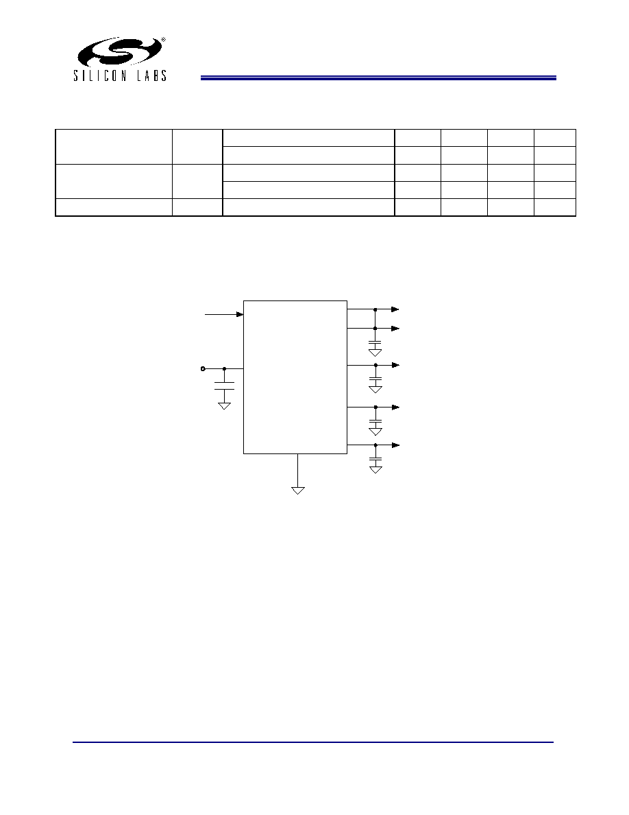
External Components & Design Considerations
Typical Application Schematic
SL23EP04
CL
0.1
μF
CLKIN
FBK
CLKA1
GND
VDD
1
7
4
3
2
8
CL
CLKA2
CL
CLKB2
CL
CLKB1
5
6
Comments and Recommendations
Decoupling Capacitor:
A decoupling capacitor of 0.1μF must be used between VDD and VSS pins. Place the
capacitor on the component side of the PCB as close to the VDD pin as possible. The PCB trace to the VDD pin and
to the GND via should be kept as short as possible. Do not use vias between the decoupling capacitor and the VDD
pin.
Series Termination Resistor: A series termination resistor is recommended if the distance between the output
clocks and the load is over 1 inch. The nominal impedance of the clock outputs is given in the Operating Condition
Tables. Place the series termination resistors as close to the clock outputs as possible.
Zero Delay and Skew Control: All outputs and CLKIN pins should be loaded with the same load to achieve “Zero
Delay” between the CLKIN and the outputs. The FBK pin is connected to PLL internally on-chip for feedback and
should be connected to one of to output clocks externally. For applications requiring zero input/output delay, the load
at the all output pins including the FBK pin must be the same. If any delay adjustment is required, the capacitance at
the FBK pin could be increased or decreased to increase or decrease the delay between Bank A and B clocks
relative to CLKIN. For minimum pin-to-pin skew, the external load at all the Bank A and B clocks must be the same.
In addition, the rise and fall time of the reference clock at CLKIN pin should be similar to rise and fall times at the
CLKA and CLK B bank outputs.
相关PDF资料 |
PDF描述 |
|---|---|
| SL23EP04SI-2T | IC BUFFER 220MHZ 4CH 3.3V 8SOIC |
| SL23EP04SI-2HT | IC BUFFER 220MHZ 4CH 3.3V 8SOIC |
| SL23EP04SI-1T | IC BUFFER 220MHZ 4CH 3.3V 8SOIC |
| SL23EP04SI-1HT | IC BUFFER 220MHZ 4CH 3.3V 8SOIC |
| ICS9179BF-03T | IC CLK BUFFER 1:10 133MHZ 28SSOP |
相关代理商/技术参数 |
参数描述 |
|---|---|
| SL23EP04SI-1H | 功能描述:时钟缓冲器 10-220MHz 4 Outputs ZDB 3.3-2.5V Hi Drv RoHS:否 制造商:Texas Instruments 输出端数量:5 最大输入频率:40 MHz 传播延迟(最大值): 电源电压-最大:3.45 V 电源电压-最小:2.375 V 最大功率耗散: 最大工作温度:+ 85 C 最小工作温度:- 40 C 封装 / 箱体:LLP-24 封装:Reel |
| SL23EP04SI-1HT | 功能描述:时钟缓冲器 10-220MHz 4 Outputs ZDB 3.3-2.5V Hi Drv RoHS:否 制造商:Texas Instruments 输出端数量:5 最大输入频率:40 MHz 传播延迟(最大值): 电源电压-最大:3.45 V 电源电压-最小:2.375 V 最大功率耗散: 最大工作温度:+ 85 C 最小工作温度:- 40 C 封装 / 箱体:LLP-24 封装:Reel |
| SL23EP04SI-1T | 功能描述:时钟缓冲器 10-220MHz 4 Outputs ZDB 3.3-2.5V RoHS:否 制造商:Texas Instruments 输出端数量:5 最大输入频率:40 MHz 传播延迟(最大值): 电源电压-最大:3.45 V 电源电压-最小:2.375 V 最大功率耗散: 最大工作温度:+ 85 C 最小工作温度:- 40 C 封装 / 箱体:LLP-24 封装:Reel |
| SL23EP04SI-2 | 功能描述:时钟缓冲器 10-220MHz 4 Outputs ZDB 3.3-2.5V RoHS:否 制造商:Texas Instruments 输出端数量:5 最大输入频率:40 MHz 传播延迟(最大值): 电源电压-最大:3.45 V 电源电压-最小:2.375 V 最大功率耗散: 最大工作温度:+ 85 C 最小工作温度:- 40 C 封装 / 箱体:LLP-24 封装:Reel |
| SL23EP04SI-2H | 功能描述:时钟缓冲器 10-220MHz 4 Outputs ZDB 3.3-2.5V Hi Drv RoHS:否 制造商:Texas Instruments 输出端数量:5 最大输入频率:40 MHz 传播延迟(最大值): 电源电压-最大:3.45 V 电源电压-最小:2.375 V 最大功率耗散: 最大工作温度:+ 85 C 最小工作温度:- 40 C 封装 / 箱体:LLP-24 封装:Reel |
发布紧急采购,3分钟左右您将得到回复。