- 您现在的位置:买卖IC网 > PDF目录98082 > SL28548ALC-2T PROC SPECIFIC CLOCK GENERATOR, QCC64 PDF资料下载
参数资料
| 型号: | SL28548ALC-2T |
| 元件分类: | 时钟产生/分配 |
| 英文描述: | PROC SPECIFIC CLOCK GENERATOR, QCC64 |
| 封装: | 9 X 9 MM, 0.50 MM PITCH, ROHS COMPLIANT, QFN-64 |
| 文件页数: | 9/32页 |
| 文件大小: | 685K |
| 代理商: | SL28548ALC-2T |
第1页第2页第3页第4页第5页第6页第7页第8页当前第9页第10页第11页第12页第13页第14页第15页第16页第17页第18页第19页第20页第21页第22页第23页第24页第25页第26页第27页第28页第29页第30页第31页第32页
SL28548-2
Rev 1.5 July 28, 2008
Page 17 of 32
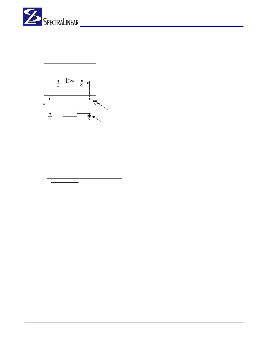
is in series with the crystal. The total capacitance on both side
is twice the specified crystal load capacitance (CL). Trim
capacitors are calculated to provide equal capacitive loading
on both sides.
,
Use the following formulas to calculate the trim capacitor
values for Ce1 and Ce2.
CL ................................................... Crystal load capacitance
CLe .........................................Actual loading seen by crystal
using standard value trim capacitors
Ce .....................................................External trim capacitors
Cs.............................................. Stray capacitance (terraced)
Ci ........................................................... Internal capacitance
(lead frame, bond wires, etc.)
Dial-A-Frequency (CPU and PCIEX)
This feature allows the user to over-clock their system by
slowly stepping up the CPU or SRC frequency. When the
programmable output frequency feature is enabled, the CPU
and SRC frequencies are determined by the following
equation:
Fcpu = G * N/M or Fcpu=G2 * N, where G2 = G / M.
“N” and “M” are the values programmed in Programmable
Frequency Select N-Value Register and M-Value Register,
respectively.
“G” stands for the PLL Gear Constant, which is determined
by the programmed value of FS[E:A]. See Table 1,
Frequency Select Table for the Gear Constant for each
Frequency selection. The PCI Express only allows user
control of the N register, the M value is fixed and
documented in Table 1, Frequency Select Table.
In this mode, the user writes the desired N and M values into
the DAF I2C registers. The user cannot change only the M
value and must change both the M and the N values at the
same time, if they require a change to the M value. The user
may change only the N value.
Associated Register Bits
CPU_DAF Enable – This bit enables CPU DAF mode. By
default, it is not set. When set, the operating frequency is
determined by the values entered into the CPU_DAF_N
register. Note that the CPU_DAF_N and M register must
contain valid values before CPU_DAF is set. Default = 0,
(No DAF).
CPU_DAF_N – There are nine bits (for 512 values) to
linearly change the CPU frequency (limited by VCO range).
Default = 0, (0000). The allowable values for N are detailed
in Table 1, Frequency Select Table.
CPU DAF M – There are 7 bits (for 128 values) to linearly
change the CPU frequency (limited by VCO range). Default
= 0, the allowable values for M are detailed in Table 1,
Frequency Select Table
SRC_DAF Enable – This bit enables SRC DAF mode. By
default, it is not set. When set, the operating frequency is
determined by the values entered into the SRC_DAF_N
register. Note that the SRC_DAF_N register must contain
valid values before SRC_DAF is set. Default = 0, (No DAF).
SRC_DAF_N – There are nine bits (for 512 values) to
linearly change the CPU frequency (limited by VCO range).
Default = 0, (0000). The allowable values for N are detailed
in Table 1, Frequency Select Table.
Smooth Switching
The device contains one smooth switch circuit that is shared
by the CPU PLL and SRC PLL. The smooth switch circuit
ensures that when the output frequency changes by
overclocking, the transition from the old frequency to the new
frequency is a slow, smooth transition containing no glitches.
The rate of change of output frequency when using the smooth
switch circuit is less than 1 MHz/0.667 s. The frequency
overshoot and undershoot is less than 2%.
The Smooth Switch circuit assigns auto or manual. In Auto
mode, clock generator assigns smooth switch automatically
when the PLL does overclocking. For manual mode, assign
the smooth switch circuit to PLL via Smbus. By default the
smooth switch circuit is set to auto mode. PLL can be
over-clocked when it does not have control of the smooth
switch circuit but it is not guaranteed to transition to the new
frequency without large frequency glitches.
Do not enable over-clocking and change the N values of both
PLLs in the same SMBUS block write and use smooth switch
mechanism on spread spectrum on/off.
PD_RESTORE
If a ‘0’ is set for Byte 0 bit 0 then, upon assertion of PWRDWN#
LOW, the SL28548-2 initiates a full reset. The result of this is
that the clock chip emulates a cold power on start and goes to
the “Latches Open” state. If the PD_RESTORE bit is set to a
‘1’ then the configuration is stored upon PWRDWN# asserted
LOW. Note that if the iAMT bit, Byte 0 bit 3, is set to a ‘1’ then
the PD_RESTORE bit must be ignored. In other words, in Intel
iAMT mode, PWRDWN# reset is not allowed.
X T A L
C e 2
C e 1
C s 1
C s 2
X 1
X 2
C i1
C i2
C lo c k C h ip
T r a c e
2 . 8 p F
T r im
3 3 p F
P in
3 t o 6 p
Figure 2. Crystal Loading Example
Load Capacitance (each side)
Total Capacitance (as seen by the crystal)
Ce = 2 * CL – (Cs + Ci)
Ce1 + Cs1 + Ci1
1
+
Ce2 + Cs2 + Ci2
1
(
)
1
=
CLe
相关PDF资料 |
PDF描述 |
|---|---|
| SL28610BLC | 100 MHz, PROC SPECIFIC CLOCK GENERATOR, QCC48 |
| SL28647CLCT | 400 MHz, PROC SPECIFIC CLOCK GENERATOR, QCC72 |
| SL28779CLCT | 133 MHz, PROC SPECIFIC CLOCK GENERATOR, QCC32 |
| SL28PCIE26ALIT | OTHER CLOCK GENERATOR, QCC32 |
| SL28PCIE26ALI | OTHER CLOCK GENERATOR, QCC32 |
相关代理商/技术参数 |
参数描述 |
|---|---|
| SL28610BLC | 功能描述:时钟发生器及支持产品 AtomPoulsbo Handheld Embed.1.5V PCIe G1 RoHS:否 制造商:Silicon Labs 类型:Clock Generators 最大输入频率:14.318 MHz 最大输出频率:166 MHz 输出端数量:16 占空比 - 最大:55 % 工作电源电压:3.3 V 工作电源电流:1 mA 最大工作温度:+ 85 C 安装风格:SMD/SMT 封装 / 箱体:QFN-56 |
| SL28610BLCT | 功能描述:时钟发生器及支持产品 AtomPoulsbo Handheld Embed.1.5V PCIe G1 RoHS:否 制造商:Silicon Labs 类型:Clock Generators 最大输入频率:14.318 MHz 最大输出频率:166 MHz 输出端数量:16 占空比 - 最大:55 % 工作电源电压:3.3 V 工作电源电流:1 mA 最大工作温度:+ 85 C 安装风格:SMD/SMT 封装 / 箱体:QFN-56 |
| SL28610BLI | 功能描述:时钟发生器及支持产品 AtomPoulsbo Handheld Embed.1.5V PCIe G1 RoHS:否 制造商:Silicon Labs 类型:Clock Generators 最大输入频率:14.318 MHz 最大输出频率:166 MHz 输出端数量:16 占空比 - 最大:55 % 工作电源电压:3.3 V 工作电源电流:1 mA 最大工作温度:+ 85 C 安装风格:SMD/SMT 封装 / 箱体:QFN-56 |
| SL28610BLIT | 功能描述:时钟发生器及支持产品 AtomPoulsbo Handheld Embed.1.5V PCIe G1 RoHS:否 制造商:Silicon Labs 类型:Clock Generators 最大输入频率:14.318 MHz 最大输出频率:166 MHz 输出端数量:16 占空比 - 最大:55 % 工作电源电压:3.3 V 工作电源电流:1 mA 最大工作温度:+ 85 C 安装风格:SMD/SMT 封装 / 箱体:QFN-56 |
| SL28610BLITR | 制造商:Silicon Laboratories Inc 功能描述: |
发布紧急采购,3分钟左右您将得到回复。