- 您现在的位置:买卖IC网 > PDF目录2017 > SL28DB200AZI (Silicon Laboratories Inc)IC CLOCK PCIE DIFF 2CH 16TSSOP PDF资料下载
参数资料
| 型号: | SL28DB200AZI |
| 厂商: | Silicon Laboratories Inc |
| 文件页数: | 3/8页 |
| 文件大小: | 0K |
| 描述: | IC CLOCK PCIE DIFF 2CH 16TSSOP |
| 标准包装: | 96 |
| 类型: | 扇出缓冲器(分配) |
| PLL: | 无 |
| 主要目的: | PCI Express(PCIe),SATA CPU |
| 输入: | 时钟 |
| 输出: | HCSL |
| 电路数: | 1 |
| 比率 - 输入:输出: | 1:2 |
| 差分 - 输入:输出: | 是/是 |
| 频率 - 最大: | 210MHz |
| 电源电压: | 3.135 V ~ 3.465 V |
| 工作温度: | -40°C ~ 85°C |
| 安装类型: | * |
| 封装/外壳: | * |
| 供应商设备封装: | * |
| 包装: | * |
SL28DB200
........................ Document #: 38-07722 Rev 0.4 Page 3 of 8
Output Enable Clarification
OE# functionality allows for enabling and disabling individual
outputs. OE1# and OE2# are Active LOW inputs. Disabling the
outputs may be implemented by deasserting the OE# input
pin. If the OE# pin is deasserted, the output of interest will be
tri-stated. (The assertion and deassertion of this signal is
absolutely asynchronous.)
OE Assertion
All differential outputs that were tri-stated will resume normal
operation in a glitch-free manner. The maximum latency from
the assertion to active outputs is between 2–6 SRC clock
periods. In addition, SRC clocks will be driven high within 15
ns of OE# assertion to a voltage greater than 200 mV
Absolute Maximum Conditions
OE Deassertion
The impact of deasserting OE# is that each corresponding
output will transition from normal operation to tri-state in a
glitch-free
manner.
The
maximum
latency
from
the
deassertion to tri-stated outputs is between 2–6 DIF clock
periods.
DC Electrical Specifications
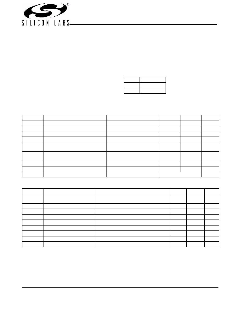
Table 2. OE Functionality
OE#
SRC,SRC#
0
Enable
1
Tri-State
Parameter
Description
Condition
Min.
Max.
Unit
VDD
Core Supply Voltage
–0.5
4.6
V
VDDA
Analog Supply Voltage
–0.5
4.6
V
VIN
Input Voltage
Relative to VSS
–0.5
VDD + 0.5
VDC
TS
Temperature, Storage
Non-functional
–65
+150
°C
TA
Temperature, Operating Ambient
(Commercial Grade)
Functional
0
85
°C
TA
Temperature, Operating Ambient
(Industrial Grade)
Functional
-40
85
°C
TJ
Temperature, Junction
Functional
150
°C
ESDHBM
ESD Protection (Human Body Model)
JEDEC (JESD 22 - A114)
2000
–
V
UL-94
Flammability Rating
UL (Class)
V–0
Parameter
Description
Condition
Min.
Max.
Unit
VDDA,
VDD
3.3V Operating Voltage
3.3 ± 5%
3.135
3.465
V
VIL
3.3V Input Low Voltage
VSS – 0.5
0.8
V
VIH
3.3V Input High Voltage
2.0
VDD + 0.5
V
IIL
Input Low Leakage Current
except internal pull-up resistors, 0 < VIN < VDD
–5
A
IIH
Input High Leakage Current
except internal pull-down resistors, 0 < VIN < VDD
5
A
CIN
Input Pin Capacitance
1.5
5
pF
COUT
Output Pin Capacitance
–-
6
pF
LIN
Pin Inductance
–
7
nH
IDD3.3V
Dynamic Supply Current
At max. load, Full Active, at 100MHz
–
60
mA
相关PDF资料 |
PDF描述 |
|---|---|
| SL28EB717ALI | IC CLK CK505 TNLCRK/TOPCLF 48QFN |
| SL28EB719AZI | IC CLK CK505 TNLCK/TPCLF 48TSSOP |
| SL28EB740AZI | IC CLK CK505 TNLCK/TPCLF 56TSSOP |
| SL28PCIE10ALI | IC CLOCK PCIE GEN2 4CH 32QFN |
| SL28PCIE14ALIT | IC CLOCK PCIE GEN2/3 BUFF 32QFN |
相关代理商/技术参数 |
参数描述 |
|---|---|
| SL28DB200AZIT | 功能描述:时钟发生器及支持产品 PCIe fam 1diff input 2 diff outputs RoHS:否 制造商:Silicon Labs 类型:Clock Generators 最大输入频率:14.318 MHz 最大输出频率:166 MHz 输出端数量:16 占空比 - 最大:55 % 工作电源电压:3.3 V 工作电源电流:1 mA 最大工作温度:+ 85 C 安装风格:SMD/SMT 封装 / 箱体:QFN-56 |
| SL28EA717ALI | 功能描述:时钟发生器及支持产品 Tunnel Creek Queen’s Bay platform RoHS:否 制造商:Silicon Labs 类型:Clock Generators 最大输入频率:14.318 MHz 最大输出频率:166 MHz 输出端数量:16 占空比 - 最大:55 % 工作电源电压:3.3 V 工作电源电流:1 mA 最大工作温度:+ 85 C 安装风格:SMD/SMT 封装 / 箱体:QFN-56 |
| SL28EA717ALIT | 功能描述:时钟发生器及支持产品 Tunnel Creek Queen’s Bay platform RoHS:否 制造商:Silicon Labs 类型:Clock Generators 最大输入频率:14.318 MHz 最大输出频率:166 MHz 输出端数量:16 占空比 - 最大:55 % 工作电源电压:3.3 V 工作电源电流:1 mA 最大工作温度:+ 85 C 安装风格:SMD/SMT 封装 / 箱体:QFN-56 |
| SL28EA719AZI | 功能描述:时钟发生器及支持产品 Tunnel Creek Queen’s Bay platform RoHS:否 制造商:Silicon Labs 类型:Clock Generators 最大输入频率:14.318 MHz 最大输出频率:166 MHz 输出端数量:16 占空比 - 最大:55 % 工作电源电压:3.3 V 工作电源电流:1 mA 最大工作温度:+ 85 C 安装风格:SMD/SMT 封装 / 箱体:QFN-56 |
| SL28EA719AZIT | 功能描述:时钟发生器及支持产品 Tunnel Creek Queen’s Bay platform RoHS:否 制造商:Silicon Labs 类型:Clock Generators 最大输入频率:14.318 MHz 最大输出频率:166 MHz 输出端数量:16 占空比 - 最大:55 % 工作电源电压:3.3 V 工作电源电流:1 mA 最大工作温度:+ 85 C 安装风格:SMD/SMT 封装 / 箱体:QFN-56 |
发布紧急采购,3分钟左右您将得到回复。