- 您现在的位置:买卖IC网 > PDF目录9615 > SL28PCIE10ALIT (Silicon Laboratories Inc)IC CLOCK PCIE GEN2 4CH 32QFN PDF资料下载
参数资料
| 型号: | SL28PCIE10ALIT |
| 厂商: | Silicon Laboratories Inc |
| 文件页数: | 16/16页 |
| 文件大小: | 0K |
| 描述: | IC CLOCK PCIE GEN2 4CH 32QFN |
| 标准包装: | 2,500 |
| 系列: | EProClock® |
| 类型: | 时钟/频率发生器 |
| PLL: | 是 |
| 主要目的: | PCI Express(PCIe) |
| 输入: | 晶体 |
| 输出: | HCSL,LVCMOS |
| 电路数: | 1 |
| 比率 - 输入:输出: | 1:7 |
| 差分 - 输入:输出: | 无/是 |
| 频率 - 最大: | 100MHz |
| 电源电压: | 3.135 V ~ 3.465 V |
| 工作温度: | -40°C ~ 85°C |
| 安装类型: | * |
| 封装/外壳: | * |
| 供应商设备封装: | * |
| 包装: | * |
SL28PCIe10
.......................................Document #: Rev 1.1 Page 9 of 16
Byte 14: Control Register 14
.
PD# (Power down) Clarification
The CK_PWRGD/PD# pin is a dual-function pin. During initial
power up, the pin functions as CK_PWRGD. Once
CK_PWRGD has been sampled HIGH by the clock chip, the
pin assumes PD# functionality. The PD# pin is an
asynchronous active LOW input used to shut off all clocks
cleanly before shutting off power to the device. This signal is
synchronized internally to the device before powering down
the clock synthesizer. PD# is also an asynchronous input for
powering up the system. When PD# is asserted LOW, clocks
are driven to a LOW value and held before turning off the
VCOs and the crystal oscillator.
PD# Assertion
When PD# has been sampled LOW by the internal reference
clock all differential clocks will be stopped in a glitch free
manner to the LOW/LOW state within their next two consec-
utive rising edges.
When PD# is sampled LOW by two consecutive cycles of an
internal reference clock, all single-ended outputs will be held
LOW on their next HIGH-to-LOW transition.
PD# Deassertion
Power up latency will be less than 2ms for crystal input
reference clock and less than 8ms for differential input
reference clock. This is the delay from the power supply
reaching the min value specified in the datasheet, until the
time that the part is ready to sample any latched inputs on the
first rising edge of CKPWRGD.
After the first rising edge on CKPWRGD this pin becomes
PD#. After a valid rising edge on CKPWRGD/PD# pin, a time
of not more than 1.8ms is allowed for the clock chip’s internal
PLL’s to power up and lock, after this time all outputs are
enabled in a glitch free manner within a few clock cycles of
each clock.
OE#_SRC2_SRC3 Assertion
The OE#_SRC2_SRC3 signal is an active LOW input used for
synchronous stopping and starting the SRC2 and SRC3
output clocks while the rest of the clock generator continues to
function. When the OE#_SRC2_SRC3 pin is asserted, all
CPU outputs that are set with the SMBus configuration to be
stoppable are stopped cleanly. The final states of the stopped
CPU signals are CPUT = HIGH and CPUC = LOW.
OE#_SRC2_SRC3 Deassertion
The deassertion of the OE#_SRC2_SRC3 signal causes all
stopped SRC2 AND SRC3 outputs to resume normal
operation in a synchronous manner. No short or stretched
clock pulses are produced when the clock resumes. The
maximum latency from the deassertion to active outputs is no
more than two SRC clock cycles.
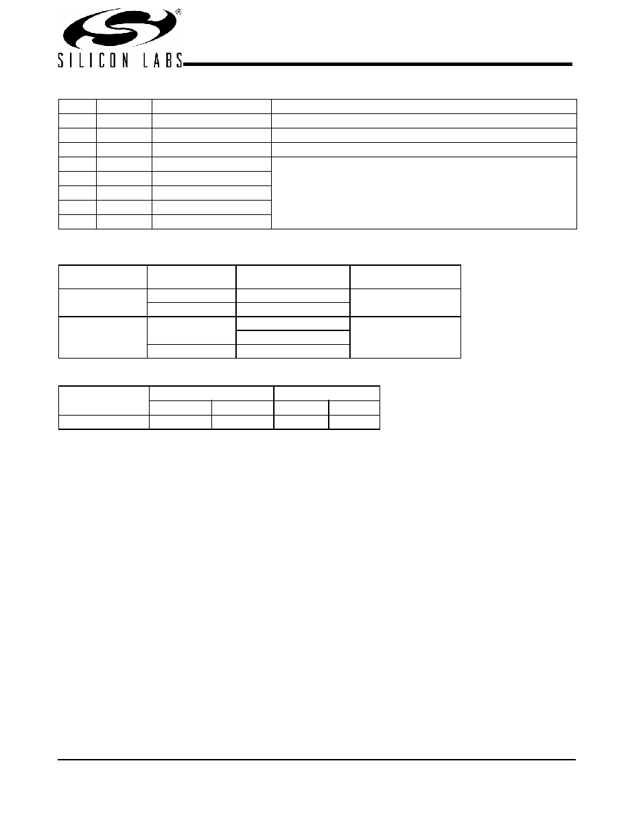
Bit
@Pup
Name
Description
7
1
RESERVED
6
0
RESERVED
5
1
RESERVED
40
OTP_4
OTP_ID
Identification for programmed device
30
OTP_3
20
OTP_2
10
OTP_1
00
OTP_0
Table 4. Output Driver Status during OE#_SRC2_SRC3
OE#_SRC2_SRC3 As-
serted
SMBus OE Disabled
Single-ended Clocks Stoppable
Running
Driven low
Non stoppable
Running
Differential Clocks
Stoppable
Clock driven high
Clock driven low
Clock# driven low
Non stoppable
Running
Table 5. Output Driver Status
All Single-ended Clocks
All Differential Clocks
w/o Strap
w/ Strap
Clock
Clock#
PD# = 0 (Power down)
Low
Hi-z
Low
相关PDF资料 |
PDF描述 |
|---|---|
| MS27505E13B22PB | CONN RCPT 22POS BOX MNT W/PINS |
| MS27484T16F26PD | CONN PLUG 26POS STRAIGHT W/PINS |
| HIN241CB-T | IC 4DRVR/5RCVR RS232 5V 28-SOIC |
| HIN241CB | IC 4DRVR/5RCVR RS232 5V 28-SOIC |
| HIN241CA | IC 4DRVR/5RCVR RS232 5V 28-SSOP |
相关代理商/技术参数 |
参数描述 |
|---|---|
| SL28PCIe14ALC | 功能描述:时钟发生器及支持产品 PCIe Stand app to PLX ref design Myra RoHS:否 制造商:Silicon Labs 类型:Clock Generators 最大输入频率:14.318 MHz 最大输出频率:166 MHz 输出端数量:16 占空比 - 最大:55 % 工作电源电压:3.3 V 工作电源电流:1 mA 最大工作温度:+ 85 C 安装风格:SMD/SMT 封装 / 箱体:QFN-56 |
| SL28PCIe14ALCT | 功能描述:时钟发生器及支持产品 PCIe Stand app to PLX ref design Myra RoHS:否 制造商:Silicon Labs 类型:Clock Generators 最大输入频率:14.318 MHz 最大输出频率:166 MHz 输出端数量:16 占空比 - 最大:55 % 工作电源电压:3.3 V 工作电源电流:1 mA 最大工作温度:+ 85 C 安装风格:SMD/SMT 封装 / 箱体:QFN-56 |
| SL28PCIe14ALI | 功能描述:时钟发生器及支持产品 PCIe Stand app to PLX ref design Myra RoHS:否 制造商:Silicon Labs 类型:Clock Generators 最大输入频率:14.318 MHz 最大输出频率:166 MHz 输出端数量:16 占空比 - 最大:55 % 工作电源电压:3.3 V 工作电源电流:1 mA 最大工作温度:+ 85 C 安装风格:SMD/SMT 封装 / 箱体:QFN-56 |
| SL28PCIe14ALIT | 功能描述:时钟发生器及支持产品 PCIe Stand app to PLX ref design Myra RoHS:否 制造商:Silicon Labs 类型:Clock Generators 最大输入频率:14.318 MHz 最大输出频率:166 MHz 输出端数量:16 占空比 - 最大:55 % 工作电源电压:3.3 V 工作电源电流:1 mA 最大工作温度:+ 85 C 安装风格:SMD/SMT 封装 / 箱体:QFN-56 |
| SL28PCIe14LC | 功能描述:时钟发生器及支持产品 Std Prod applicable PLX ref design Myra RoHS:否 制造商:Silicon Labs 类型:Clock Generators 最大输入频率:14.318 MHz 最大输出频率:166 MHz 输出端数量:16 占空比 - 最大:55 % 工作电源电压:3.3 V 工作电源电流:1 mA 最大工作温度:+ 85 C 安装风格:SMD/SMT 封装 / 箱体:QFN-56 |
发布紧急采购,3分钟左右您将得到回复。