- 您现在的位置:买卖IC网 > PDF目录9046 > SL28SRC01BZIT (Silicon Laboratories Inc)IC CLOCK PCIE GEN3/2 DIF 16TSSOP PDF资料下载
参数资料
| 型号: | SL28SRC01BZIT |
| 厂商: | Silicon Laboratories Inc |
| 文件页数: | 4/11页 |
| 文件大小: | 0K |
| 描述: | IC CLOCK PCIE GEN3/2 DIF 16TSSOP |
| 标准包装: | 2,500 |
| 类型: | * |
| PLL: | 是 |
| 输入: | 时钟,晶体 |
| 输出: | 时钟 |
| 电路数: | 1 |
| 比率 - 输入:输出: | 1:1 |
| 差分 - 输入:输出: | 无/是 |
| 频率 - 最大: | 100MHz |
| 除法器/乘法器: | 无/无 |
| 电源电压: | 3.135 V ~ 3.465 V |
| 工作温度: | -40°C ~ 85°C |
| 安装类型: | * |
| 封装/外壳: | * |
| 供应商设备封装: | * |
| 包装: | * |
SL28SRC01
DOC#: SP-AP-0015 (Rev. 0.2)
Page 2 of 11
Pin Definitions
The SL28SRC01 requires a Parallel Resonance Crystal.
Substituting a series resonance crystal causes the
SL28SRC01 to operate at the wrong frequency and violates
the ppm specification. For most applications there is a
300-ppm frequency shift between series and parallel crystals
due to incorrect loading.
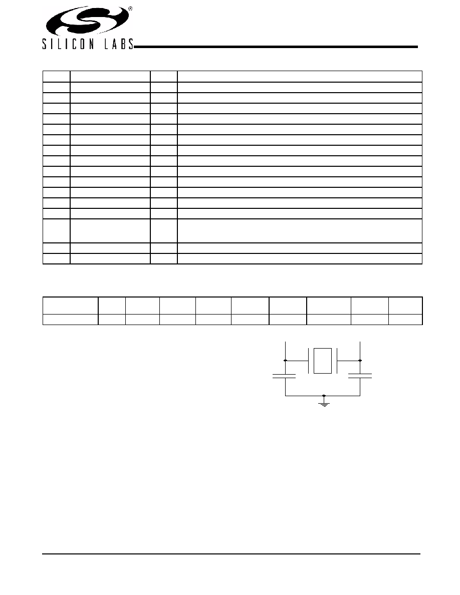
Crystal Loading
Crystal loading plays a critical role in achieving low ppm perfor-
mance. To realize low ppm performance, use the total capac-
itance the crystal sees to calculate the appropriate capacitive
loading (CL).
shows a typical crystal configuration using the two
trim capacitors. It is important that the trim capacitors are in
series with the crystal. It is not true that load capacitors are in
parallel with the crystal and are approximately equal to the
load capacitance of the crystal.
Calculating Load Capacitors
In addition to the standard external trim capacitors, consider
the trace capacitance and pin capacitance to calculate the
crystal loading correctly. Again, the capacitance on each side
is in series with the crystal. The total capacitance on both side
is twice the specified crystal load capacitance (CL). Trim
Pin No.
Name
Type
Description
1
XIN
I
14.318 MHz Crystal input.
2
VDD
PWR 3.3V power supply
3
VDD
PWR 3.3V power supply
4
VSS
GND
Ground
5
VDD
PWR 3.3V power supply
6
VSS
GND
Ground
7
SRC1
O, DIF 100 MHz Differential serial reference clocks.
8
SRC1#
O, DIF 100 MHz Differential serial reference clocks.
9
VSS
GND
Ground
10
VDD
PWR 3.3V power supply
11
VDD
PWR 3.3V power supply
12
VSS
GND
Ground
13
VDD
PWR 3.3V power supply
14
SSON
I
3.3V LVTTL input for enabling spread spectrum clock
0 = Disable, 1 = Enable (-0.5% SS)
Extrenal 10K ohm pull-up or pull-down resistor required
15
VSS
GND
Ground
16
XOUT
O
14.318 MHz Crystal output.
Table 1. Crystal Recommendations
Frequency
(Fund)
Cut
Loading
Load Cap
Drive
(max.)
Shunt Cap
(max.)
Motional
(max.)
Tolerance
(max.)
Stability
(max.)
Aging
(max.)
14.31818 MHz
AT
Parallel
20 pF
0.1 mW
5 pF
0.016 pF
35 ppm
30 ppm
5 ppm
Figure 1. Crystal Capacitive Clarification
相关PDF资料 |
PDF描述 |
|---|---|
| VE-JWL-MZ-F4 | CONVERTER MOD DC/DC 28V 25W |
| ICS91718CMT | IC CLOCK GENERATOR LOW EMI 8SOIC |
| ICS91718CMLFT | IC CLOCK GENERATOR LOW EMI 8SOIC |
| ICS552AR-01LFT | IC OSC/MULT/BUFFER OCT 20-SSOP |
| ICS91309AGILFT | IC CLK BUFFER ZD PLL 16TSSOP |
相关代理商/技术参数 |
参数描述 |
|---|---|
| SL28SRC02BZC | 功能描述:时钟发生器及支持产品 PCIE Clk Gen 14.318M Xin 2PCIE out Gen3 RoHS:否 制造商:Silicon Labs 类型:Clock Generators 最大输入频率:14.318 MHz 最大输出频率:166 MHz 输出端数量:16 占空比 - 最大:55 % 工作电源电压:3.3 V 工作电源电流:1 mA 最大工作温度:+ 85 C 安装风格:SMD/SMT 封装 / 箱体:QFN-56 |
| SL28SRC02BZCT | 功能描述:时钟发生器及支持产品 PCIE Clk Gen 14.318M Xin 2PCIE out Gen3 RoHS:否 制造商:Silicon Labs 类型:Clock Generators 最大输入频率:14.318 MHz 最大输出频率:166 MHz 输出端数量:16 占空比 - 最大:55 % 工作电源电压:3.3 V 工作电源电流:1 mA 最大工作温度:+ 85 C 安装风格:SMD/SMT 封装 / 箱体:QFN-56 |
| SL28SRC02BZCTR | 制造商:Silicon Laboratories Inc 功能描述: |
| SL28SRC02BZI | 功能描述:时钟发生器及支持产品 PCIE Clk Gen Xin 14M -->4 PCIE out Gen3 RoHS:否 制造商:Silicon Labs 类型:Clock Generators 最大输入频率:14.318 MHz 最大输出频率:166 MHz 输出端数量:16 占空比 - 最大:55 % 工作电源电压:3.3 V 工作电源电流:1 mA 最大工作温度:+ 85 C 安装风格:SMD/SMT 封装 / 箱体:QFN-56 |
| SL28SRC02BZIT | 功能描述:时钟发生器及支持产品 PCIE Clk Gen Xin 14M -->4 PCIE out Gen3 RoHS:否 制造商:Silicon Labs 类型:Clock Generators 最大输入频率:14.318 MHz 最大输出频率:166 MHz 输出端数量:16 占空比 - 最大:55 % 工作电源电压:3.3 V 工作电源电流:1 mA 最大工作温度:+ 85 C 安装风格:SMD/SMT 封装 / 箱体:QFN-56 |
发布紧急采购,3分钟左右您将得到回复。