- 您现在的位置:买卖IC网 > PDF目录98084 > SM320C6416DGADW60 (TEXAS INSTRUMENTS INC) 64-BIT, 75 MHz, OTHER DSP, CPGA570 PDF资料下载
参数资料
| 型号: | SM320C6416DGADW60 |
| 厂商: | TEXAS INSTRUMENTS INC |
| 元件分类: | 数字信号处理 |
| 英文描述: | 64-BIT, 75 MHz, OTHER DSP, CPGA570 |
| 封装: | 33 X 33 MM, CERAMIC, FCPGA-570 |
| 文件页数: | 84/134页 |
| 文件大小: | 1997K |
| 代理商: | SM320C6416DGADW60 |
第1页第2页第3页第4页第5页第6页第7页第8页第9页第10页第11页第12页第13页第14页第15页第16页第17页第18页第19页第20页第21页第22页第23页第24页第25页第26页第27页第28页第29页第30页第31页第32页第33页第34页第35页第36页第37页第38页第39页第40页第41页第42页第43页第44页第45页第46页第47页第48页第49页第50页第51页第52页第53页第54页第55页第56页第57页第58页第59页第60页第61页第62页第63页第64页第65页第66页第67页第68页第69页第70页第71页第72页第73页第74页第75页第76页第77页第78页第79页第80页第81页第82页第83页当前第84页第85页第86页第87页第88页第89页第90页第91页第92页第93页第94页第95页第96页第97页第98页第99页第100页第101页第102页第103页第104页第105页第106页第107页第108页第109页第110页第111页第112页第113页第114页第115页第116页第117页第118页第119页第120页第121页第122页第123页第124页第125页第126页第127页第128页第129页第130页第131页第132页第133页第134页
SMJ320C6414, SMJ320C6415, SMJ320C6416
FIXEDPOINT DIGITAL SIGNAL PROCESSORS
SGUS050A JANUARY 2004 REVISED MARCH 2004
53
POST OFFICE BOX 1443
HOUSTON, TEXAS 772511443
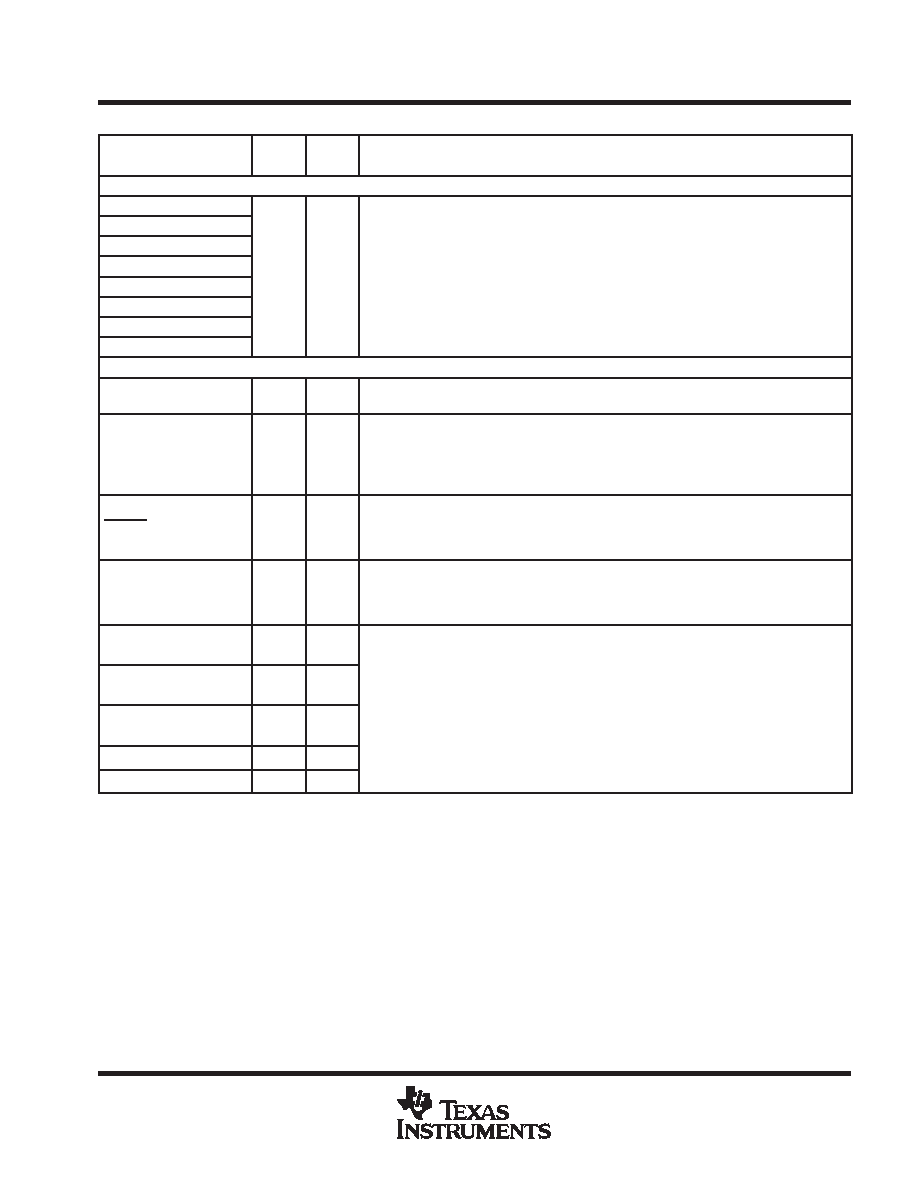
Terminal Functions (Continued)
SIGNAL
TYPE
IPD/
DESCRIPTION
NAME
NO.
TYPE
IPD/
IPU
DESCRIPTION
UTOPIA SLAVE (ATM CONTROLLER) TRANSMIT INTERFACE (CONTINUED)
UXDATA7Y
W10
UXDATA6Y
T11
UXDATA5Y
W9
8-bit Transmit Data Bus
Using the Transmit Data Bus, the UTOPIA Slave (on the rising edge of the UXCLK) transmits
UXDATA4Y
AB6
O/Z
8-bit Transmit Data Bus
Using the Transmit Data Bus, the UTOPIA Slave (on the rising edge of the UXCLK) transmits
the 8-bit ATM cells to the Master ATM Controller.
UXDATA3Y
V10
O/Z
the 8-bit ATM cells to the Master ATM Controller.
When the UTOPIA peripheral is disabled (UTOPIA_EN [BEA11 pin] = 0), these pins are tied-
UXDATA2Y
U10
When the UTOPIA peripheral is disabled (UTOPIA_EN [BEA11 pin] = 0), these pins are tied-
off.
UXDATA1Y
AA7
off.
UXDATA0Y
V9
UTOPIA SLAVE (ATM CONTROLLER) RECEIVE INTERFACE
URCLKY
U12
I
h
Source clock for UTOPIA receive driven by Master ATM Controller.
When the UTOPIA peripheral is disabled (UTOPIA_EN [BEA11 pin] = 0), this pin is tied-off.
URCLAVY
AA14
O/Z
Receive cell available status output signal from UTOPIA Slave.
0
indicates NO space is available to receive a cell from Master ATM Controller
1
indicates space is available to receive a cell from Master ATM Controller
When the UTOPIA peripheral is disabled (UTOPIA_EN [BEA11 pin] = 0), this pin is tied-off.
URENBY
AB16
I
UTOPIA receive interface enable input signal. Asserted by the Master ATM Controller to indi-
cate to the UTOPIA Slave to sample the Receive Data Bus (URDATA[7:0]) and URSOC signal
in the next clock cycle or thereafter.
When the UTOPIA peripheral is disabled (UTOPIA_EN [BEA11 pin] = 0), this pin is tied-off.
URSOCY
W13
I
h
Receive Start-of-Cell signal. This signal is output by the Master ATM Controller to indicate to
the UTOPIA Slave that the first valid byte of the cell is available to sample on the 8-bit Receive
Data Bus (URDATA[7:0]).
When the UTOPIA peripheral is disabled (UTOPIA_EN [BEA11 pin] = 0), this pin is tied-off.
CLKX1/
URADDR4§
T12
I/O/Z
McBSP1 [default] or UTOPIA receive address pins
As UTOPIA receive address pins URADDR[4:0] (I), UTOPIA_EN (BEA11 pin) = 1:
CLKS1/
URADDR3§
Y8
I
As UTOPIA receive address pins URADDR[4:0] (I), UTOPIA_EN (BEA11 pin) = 1:
5-bit Slave receive address input pins driven by the Master ATM Controller to identify and
select one of the Slave devices (up to 31 possible) in the ATM System.
CLKR1/
URADDR2§
AB7
I/O/Z
select one of the Slave devices (up to 31 possible) in the ATM System.
URADDR1 and URADDR0 pins are tied off when the UTOPIA peripheral is disabled
[UTOPIA_EN (BEA11 pin) = 0]
URADDR1Y
U11
I
[UTOPIA_EN (BEA11 pin) = 0]
For the McBSP1 pin functions (UTOPIA_EN (BEA11 pin) = 0 [default]), see the MULTICHAN-
URADDR0Y
AA9
I
For the McBSP1 pin functions (UTOPIA_EN (BEA11 pin) = 0 [default]), see the MULTICHAN-
NEL BUFFERED SERIAL PORT 1 (McBSP1) section of this table.
I = Input, O = Output, Z = High impedance, S = Supply voltage, GND = Ground
IPD = Internal pulldown, IPU = Internal pullup. (These IPD/IPU signal pins feature a 30-k IPD or IPU resistor. To pull up a signal to the opposite
supply rail, a 1-k
resistor should be used.)
§ These pins are multiplexed pins. For more details, see the Device Configurations section of this data sheet.
hExternal pulldowns required: If UTOPIA is selected (BEA11 = 1) and these pins are connected to other devices, then a 10-k resistor must be
used to externally pull down each of these pins. If these pins are “no connects”, then only UXCLK and URCLK need to be pulled down and other
pulldowns are not necessary.
External pullups required: If UTOPIA is selected (BEA11 = 1) and these pins are connected to other devices, then a 10-k resistor must be used
to externally pull up each of these pins. If these pins are “no connects”, then the pullups are not necessary.
ΨThe C6414 device does not support the UTOPIA peripheral; therefore, these standalone UTOPIA pins are Reserved (leave unconnected, do
not connect to power or ground) with the exception of UXCLK and URCLK which should be connected to a 10-k
pulldown resistor (see the
square [
h] footnote).
相关PDF资料 |
PDF描述 |
|---|---|
| SMJ320C6701GLPW16 | 32-BIT, 166.66 MHz, OTHER DSP, CBGA429 |
| SMJ34010-50FDM | GRAPHICS PROCESSOR, CQCC68 |
| SMJ34010-40GBM | GRAPHICS PROCESSOR, CPGA68 |
| SMJ34010FDM | GRAPHICS PROCESSOR, CQCC68 |
| SMJ9914AFDS | IEEE 488 (GPIB) BUS CONTROLLER, CQCC44 |
相关代理商/技术参数 |
参数描述 |
|---|---|
| SM320C6424GDUQ6EP | 功能描述:数字信号处理器和控制器 - DSP, DSC EP Fixed-Pt Dig Signal Proc RoHS:否 制造商:Microchip Technology 核心:dsPIC 数据总线宽度:16 bit 程序存储器大小:16 KB 数据 RAM 大小:2 KB 最大时钟频率:40 MHz 可编程输入/输出端数量:35 定时器数量:3 设备每秒兆指令数:50 MIPs 工作电源电压:3.3 V 最大工作温度:+ 85 C 封装 / 箱体:TQFP-44 安装风格:SMD/SMT |
| SM320C6455BGTZEP | 功能描述:数字信号处理器和控制器 - DSP, DSC Enh Product Fixed- Pt Dig Signal Proc RoHS:否 制造商:Microchip Technology 核心:dsPIC 数据总线宽度:16 bit 程序存储器大小:16 KB 数据 RAM 大小:2 KB 最大时钟频率:40 MHz 可编程输入/输出端数量:35 定时器数量:3 设备每秒兆指令数:50 MIPs 工作电源电压:3.3 V 最大工作温度:+ 85 C 封装 / 箱体:TQFP-44 安装风格:SMD/SMT |
| SM320C6455BGTZSEP | 功能描述:数字信号处理器和控制器 - DSP, DSC Enh Product Fixed- Pt Dig Signal Proc RoHS:否 制造商:Microchip Technology 核心:dsPIC 数据总线宽度:16 bit 程序存储器大小:16 KB 数据 RAM 大小:2 KB 最大时钟频率:40 MHz 可编程输入/输出端数量:35 定时器数量:3 设备每秒兆指令数:50 MIPs 工作电源电压:3.3 V 最大工作温度:+ 85 C 封装 / 箱体:TQFP-44 安装风格:SMD/SMT |
| SM320C6455-EP | 制造商:TI 制造商全称:Texas Instruments 功能描述:FIXED-POINT DIGITAL SIGNAL PROCESSOR |
| SM320C6472EGTZA6 | 功能描述:数字信号处理器和控制器 - DSP, DSC Fixed-Pt Dig Sig Proc RoHS:否 制造商:Microchip Technology 核心:dsPIC 数据总线宽度:16 bit 程序存储器大小:16 KB 数据 RAM 大小:2 KB 最大时钟频率:40 MHz 可编程输入/输出端数量:35 定时器数量:3 设备每秒兆指令数:50 MIPs 工作电源电压:3.3 V 最大工作温度:+ 85 C 封装 / 箱体:TQFP-44 安装风格:SMD/SMT |
发布紧急采购,3分钟左右您将得到回复。