- 您现在的位置:买卖IC网 > PDF目录299913 > SM5520TS-FREQ2 (PLETRONICS INC) CRYSTAL OSCILLATOR, CLOCK, 33 MHz - 50 MHz, CMOS OUTPUT PDF资料下载
参数资料
| 型号: | SM5520TS-FREQ2 |
| 厂商: | PLETRONICS INC |
| 元件分类: | XO, clock |
| 英文描述: | CRYSTAL OSCILLATOR, CLOCK, 33 MHz - 50 MHz, CMOS OUTPUT |
| 文件页数: | 1/1页 |
| 文件大小: | 44K |
| 代理商: | SM5520TS-FREQ2 |
SM5545T CMOS Series
4 Pad 5x 3.2mm Leadless Surface Mount Ceramic Clock Oscillator
CMOS with Enable/ Disable
Fundamental or 3rd Overtone Crystal Used
2.500 MHz – 125.000 MHz
Standard Specifications
Overall Frequency Stability
SM5545T: ± 50 PPM, SM5544T:
± 25 PPM, SM5520T: ± 20 PPM over Operating Temp. Range
Operating Temperature Range
Supply Voltage (Vcc)
5.0 volts and 3.3 volts available, .01 F bypass cap recommended
Symmetry (Duty Cycle)
40/60 to 60/40% is standard, but 45/55% at 50% of Vcc is also available (see Waveform 1)
Output Load
Standard load is 15 pF (typ. 1 ASIC) maximum, see Test Circuit 2 (consult factory for heavier loads)
Enable/Disable Option (E/D)
Output enabled when Pin #1 is open or at Logic “1”; Output disabled when Pin #1 is at Logic “0”.
Rise and Fall Time (Tr & Tf)
10 nS maximum
Frequency Range
(MHz)
2.500 – 33.000
12
20
33.000 – 50.000
25
45
50.000 – 70.000
35
50
70.000 – 125.00
60
100
Part Numbering Guide
Model
Frequency Stability
45 = ± 50 PPM
44 = ± 25 PPM
SM55 45 T V - 50.0M - 30 - XXX (Internal Code or blank)
Consult factory for available frequencies and specs. Not all options available for all frequencies. A special part number may be assigned.
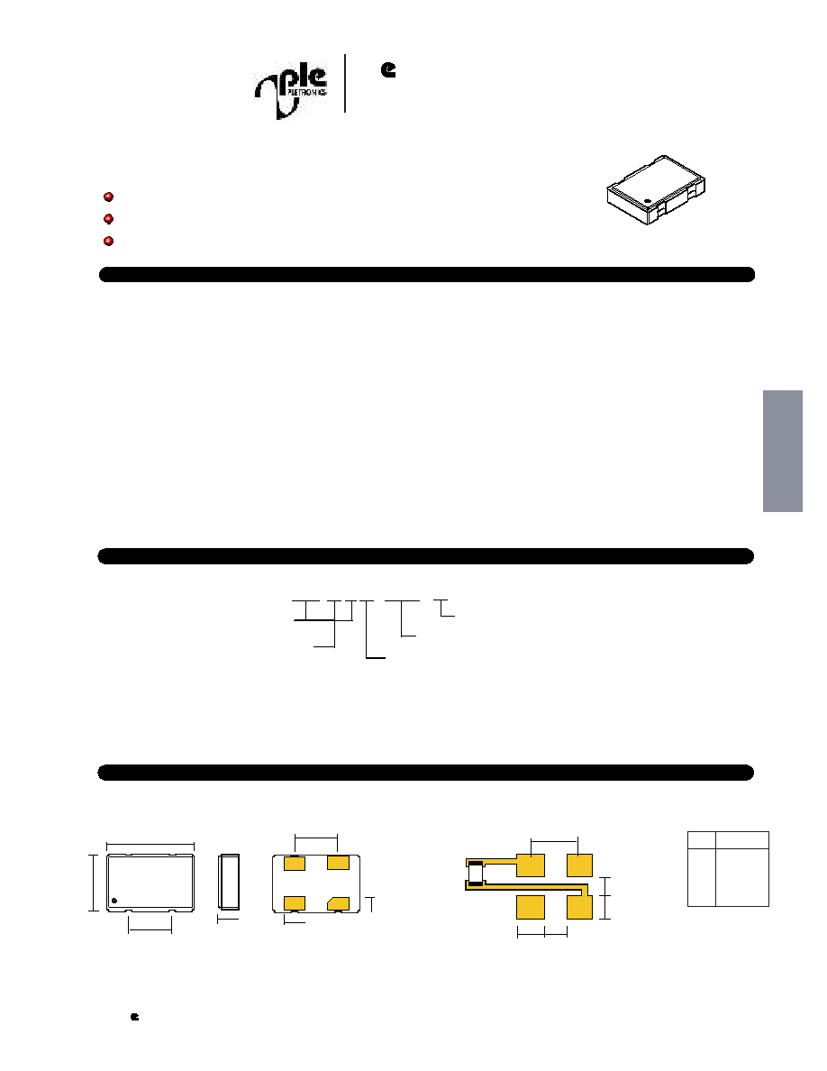
Mechanical:
not to scale
inches (mm)
Solder Pads
Jun 2004
0 to +70°C is standard, but can be extended to - 40 to +85°C for certain frequencies
(425) 776 -1880, Fax: (425) 776-2760, ple-sales@pletronics.com, www.pletronics.com
13
Pl tronics, Inc.
Frequency Stability is inclusive of frequency shifts due to calibration, temperature, supply voltage, shock, vibration and load
Packaging
Tray or
16mm tape
8mm pitch
Due to part size and factory abilities, part marking may vary from lot to lot and may contain our part number or an internal code.
Frequency in MHz
Special Specifications (choose all that apply)
°
Y: Std Specs (5.0V ± 10%, 0 to +70 C, 40/60% Symmetry)
E: Extended Operating Temperature Range (- 40 to +85 C)
S: 45/55% Symmetry at 50% of Vcc
V: Supply Voltage of 3.3 volts ±10%
Non-Std Output Load
20 = ± 20 PPM
Logic Levels
Logic “1” 90% of Vcc MIN; Logic “0” 10% of Vcc MAX
Pl tronics, Inc.
19013 36th Ave. W, Suite H Lynnwood, WA 98036 USA
Manufacturer of High Quality Frequency Control Products
.
CMOS
<
80
MHz
Page
11A
-
16
Portions of the part number that appear after the frequency may not be marked on part (C of C provided)
Blank = 15 pF max, 30 = 30 pF max
Max. Supply Current
Icc (mA) w/ 15pF load
3.3V
5.0V
m
.01 F
bypass
capacitor
MAX
0.100 (2.54)
0.047 (1.2)
0.197 (5.0 ± .15)
0.126
(3.2
±
.15)
0.047
(1.2)
0.039
(1.0)
1
4
1
2
3
4
0.100 (2.54)
0.059 (1.5)
0.032 (0.8)
0.063
(1.6)
0.037
(0.93)
3
2
1
E/D
2
GND
3
OUT
4
Vcc
PIN
SIGNAL
0.100 (2.54)
Due to part size and factory abilities, part marking may vary from lot to lot
and may contain our part number or an internal code.
m
.01 F
bypass
capacitor
MAX
0.100 (2.54)
0.047 (1.2)
0.197 (5.0 ± .15)
0.126
(3.2
±
.15)
0.047
(1.2)
0.039
(1.0)
1
4
1
2
3
4
0.100 (2.54)
0.059 (1.5)
0.032 (0.8)
0.063
(1.6)
0.037
(0.93)
3
2
1
E/D
2
GND
3
OUT
4
Vcc
PIN
SIGNAL
0.100 (2.54)
P5XYWWE
14.318MV
Marking Example and Explanation
P = Pletronics
5 = Package Code
X = Frequency Stability
YWW = Date Code
Frequency in MHz
E = Applicable Specs (some internal)
V = Applicable Specs (continued)
相关PDF资料 |
PDF描述 |
|---|---|
| SM5544MY-FREQ-T500 | CRYSTAL OSCILLATOR, CLOCK, 0.8 MHz - 80 MHz, CMOS OUTPUT |
| SM5545TEV-25.0M | OSC 3.3V SMT 5X3 CMOS |
| SM5545TSV-25.0M | OSC 3.3V SMT 5X3 CMOS |
| SM5545TEV-66.667M | OSC 3.3V SMT 5X3 CMOS |
| SM7620DESB-FREQ | CRYSTAL OSCILLATOR, CLOCK, 70 MHz - 135 MHz, CMOS OUTPUT |
相关代理商/技术参数 |
参数描述 |
|---|---|
| SM5520TSV-20.0M-30 | 制造商:Pletronics 功能描述:CMOS 3.2X5 OSC 20PPM 3.3V__Contact Local Pletronics Rep |
| SM5520TSV-25.0M-30 | 制造商:Pletronics 功能描述:CMOS 3.2X5 OSC 20PPM 3.3V__Contact Local Pletronics Rep |
| SM5520TSV-26.0M | 制造商:Pletronics 功能描述:CMOS 3.2X5 OSC 20PPM 3.3V__Contact Local Pletronics Rep |
| SM5520TSV-48.0M-SB | 制造商:Pletronics 功能描述:CMOS 3.2X5 OSC 20PPM 3.3V__Contact Local Pletronics Rep |
| SM5520TV | 制造商:PLETRONICS 制造商全称:Pletronics, Inc. 功能描述:3.3 V CMOS Clock Oscillators |
发布紧急采购,3分钟左右您将得到回复。