- 您现在的位置:买卖IC网 > PDF目录5708 > SMP08FSZ-REEL (Analog Devices Inc)IC AMP SAMPLE HOLD OCTAL 16SOIC PDF资料下载
参数资料
| 型号: | SMP08FSZ-REEL |
| 厂商: | Analog Devices Inc |
| 文件页数: | 6/8页 |
| 文件大小: | 0K |
| 描述: | IC AMP SAMPLE HOLD OCTAL 16SOIC |
| 标准包装: | 2,500 |
| 放大器类型: | 采样和保持 |
| 电路数: | 8 |
| 转换速率: | 4 V/µs |
| 电流 - 输入偏压: | 500nA |
| 电压 - 输入偏移: | 2500µV |
| 电流 - 电源: | 6mA |
| 电流 - 输出 / 通道: | 1.2mA |
| 电压 - 电源,单路/双路(±): | 5 V ~ 12 V,±2.5 V ~ 6 V |
| 工作温度: | -40°C ~ 85°C |
| 安装类型: | 表面贴装 |
| 封装/外壳: | 16-SOIC(0.154",3.90mm 宽) |
| 供应商设备封装: | 16-SOIC |
| 包装: | 带卷 (TR) |
SMP08
–6–
REV. D
14
13
12
11
16
15
10
9
8
1
2
3
4
7
6
5
SMP08
R2
10k
R2
10k
R2
10k
R2
10k
R3
6.5k
R4
1k
R1
10
D1
C1
10F
C2
1F
+
VCC
+15V
R2
10k
R2
10k
R2
10k
R2
10k
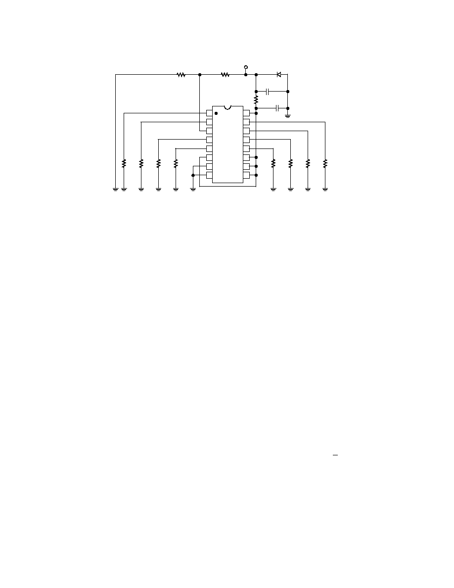
Figure 17. Burn-In Circuit
OUTPUT BUFFERS (Pins 1, 2, 4, 5, 12, 13, 14, 15)
The buffer offset specification is 10 mV; this is less than 1/2 LSB
of an 8-bit DAC with 10 V full scale. The hold step (magni-
tude of step caused in the output voltage when switching from
sample-to-hold mode, also referred to as the pedestal error or
sample-to-hold offset), is about 2.5 mV with little variation
over the full output voltage range, TA = +25
°C to +85°C. The
droop rate of a held channel is 2 mV/s typical and 20 mV/s
maximum.
The buffers are designed to drive loads connected to ground.
The outputs can source more than 20 mA, over the full voltage
range, but have limited current sinking capability near VSS. In
split supply operation, symmetrical output swings can be ob-
tained by restricting the output range to 2 V from either supply.
On-chip SMP08 buffers eliminate potential stability problems
associated with external buffers; outputs are stable with ca-
pacitive loads up to 500 pF. However, since the SMP08’s
buffer outputs are not short-circuit protected, care should be
taken to avoid shorting any output to the supplies or ground.
SIGNAL INPUT (Pin 3)
The signal input should be driven from a low impedance volt-
age source such as the output of an op amp. The op amp
should have a high slew rate and fast settling time if the
SMP08’s acquisition time characteristics are to be maintained.
As with all CMOS devices, all input voltages should be kept
within range of the supply rails (VSS < VIN < VDD) to avoid the
possibility of latchup. If single supply operation is desired, op
amps such as the OP183 or AD820 that have input and output
voltage compliances including ground, can be used to drive the
inputs. Split supplies, such as
±7.5 V, can be used with the
SMP08.
APPLICATION TIPS
All unused digital inputs should be connected to logic LOW
and unused analog inputs connected to analog ground. For
connector-driven analog inputs that may become temporarily
disconnected, a resistor to VDD, VSS or analog ground should
be used with a value ranging from 200 k
to 1 M.
APPLICATIONS INFORMATION
The SMP08, a multiplexed octal S/H, minimizes board space in
systems requiring cycled calibration or an array of control volt-
ages. When used in conjunction with a low cost 16-bit D/A, the
SMP08 can easily be integrated into microprocessor based sys-
tems. Since the SMP08 features break-before-make switching
and an internal decoder, no external logic is required. The
SMP08 has an internally regulated TTL supply so that TTL/
CMOS compatibility is maintained over the full supply range.
See Figure 18 for channel decode address information.
POWER SUPPLIES
The SMP08 is capable of operating with either single or dual
supplies, over a voltage range of 7 volts to 15 volts. Based on the
supply voltages chosen, VDD and VSS establish the input and
output voltage range, which is:
(VSS +0.06 V) ≤ VOUT/IN ≤ (VDD –2 V)
Note that several specifications, including acquisition time, off-
set and output voltage compliance, will degrade for supply volt-
ages of less than 7 V.
If split supplies are used, the negative supply should be bypassed
with a 0.1
F capacitor in parallel with a 10 F to ground. The
internal hold capacitors are connected to this supply pin and any
noise will appear at the outputs.
In single supply applications, it is extremely important that the
VSS (negative supply) pin is connected to a clean ground. The
hold capacitors are internally tied to the VSS (negative) rail. Any
ground noise or disturbance will directly couple to the output of
the sample-and-hold, degrading the signal-to-noise perfor-
mance. The analog and digital ground traces on the circuit
board should be physically separated to reduce digital switching
noise from entering the analog circuitry.
POWER SUPPLY SEQUENCING
VDD should be applied to the SMP08 before the logic input sig-
nals. The SMP08 has been designed to be immune to latchup,
but standard precautions should still be taken.
相关PDF资料 |
PDF描述 |
|---|---|
| 925306-3 | CONN TAB HSG .312 3POS BLACK |
| LT1058ACN | IC PREC OP-AMP JFET QUAD 14-DIP |
| MCP6442T-E/MS | IC OPAMP DUAL 1.6V 9KHZ 8MSOP |
| RC0201JR-0711KL | RES 11K OHM 1/20W 5% 0201 SMD |
| MCP6S91-E/P | IC PGA 1CH R-R I/O SPI 8DIP |
相关代理商/技术参数 |
参数描述 |
|---|---|
| SMP-08V-BC | 功能描述:CONN SM 8POS CRIMP 2.5MM RoHS:是 类别:连接器,互连式 >> 矩形 - 外壳 系列:SM 标准包装:1,000 系列:* 其它名称:0039-01-8019003901-801939-01-801939018019 |
| SMP-08V-NC | 制造商:JST Manufacturing 功能描述:Conn Housing RCP 8 POS 2.5mm Crimp ST Cable Mount Bag |
| SMP0900SCMC | 功能描述:THYRISTOR 90V 400A SMB 制造商:stmicroelectronics 系列:SMP,TRISIL? 包装:剪切带(CT) 零件状态:有效 电压 - 导通:98V 电压 - 断态:90V 电压 - 通态:3V 电流 - 峰值脉冲(8/20μs):400A 电流 - 峰值脉冲(10/1000μs):100A 电流 - 保持(Ih):150mA 元件数:1 电容:80pF 封装/外壳:DO-214AA,SMB 标准包装:1 |
| SMP-09V-BC | 制造商:JST Manufacturing 功能描述:9 1 Housing vO 23mm 250VDC / 250VAC 3A 85 -25 22-28AWG 11.7mm 7.4mm 制造商:JST Manufacturing 功能描述:Connector,Plastic Housing Lance,Multipo |
| SMP-09V-NC | 制造商:JST Manufacturing 功能描述:Conn Housing RCP 9 POS 2.5mm Crimp ST Cable Mount Bag |
发布紧急采购,3分钟左右您将得到回复。