- 您现在的位置:买卖IC网 > PDF目录54482 > SMS7623-108 (SKYWORKS SOLUTIONS INC) SILICON, MIXER DIODE PDF资料下载
参数资料
| 型号: | SMS7623-108 |
| 厂商: | SKYWORKS SOLUTIONS INC |
| 元件分类: | 射频混频器 |
| 英文描述: | SILICON, MIXER DIODE |
| 封装: | HERMETIC SEALED PACKAGE-1 |
| 文件页数: | 1/8页 |
| 文件大小: | 820K |
| 代理商: | SMS7623-108 |
Skyworks Solutions, Inc. Phone [781] 376-3000 Fax [781] 376-3100 sales@skyworksinc.com www.skyworksinc.com
200847 Rev. A Skyworks Proprietary Information Products and Product Information are Subject to Change Without Notice. October 3, 2008
1
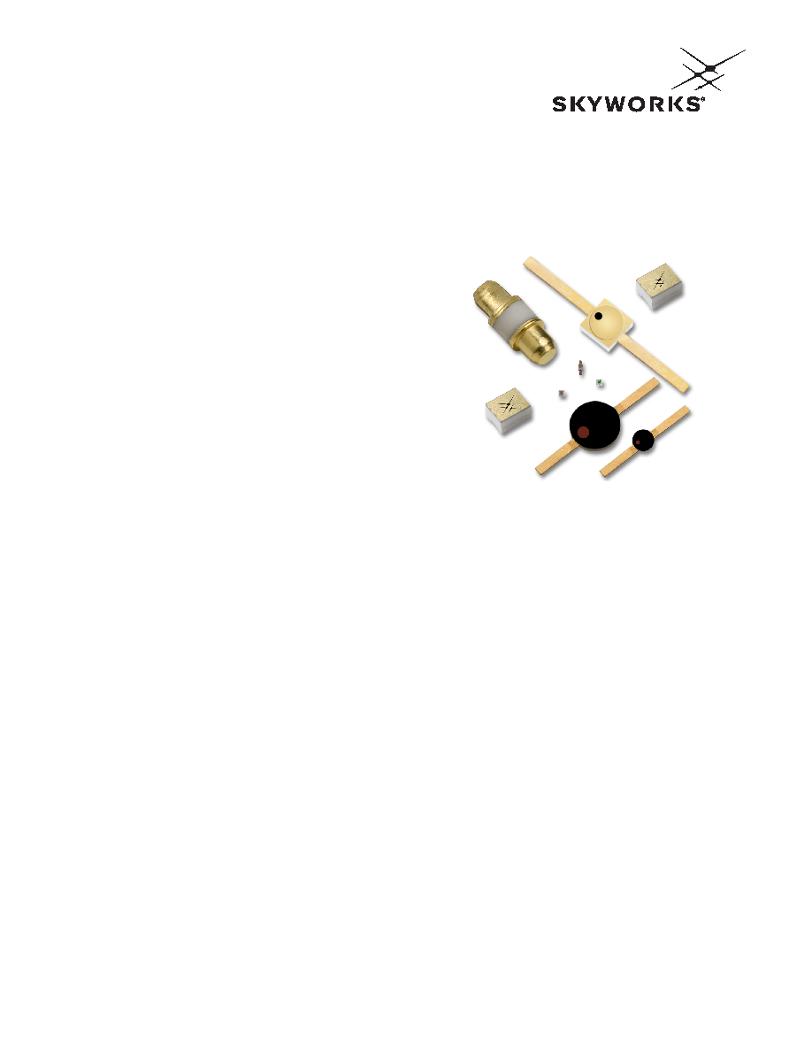
Silicon Schottky Barrier Diodes: Packaged, Bondable Chips
and Beam-Leads
data sheet
Applications
l
Detectors
Features
l
Both P-type and N-type low barrier silicon available
l
Low 1/f noise
l
Bonded junctions for reliability
l
Planar passivated beam-lead and chip construction
l
See also zero bias silicon schottky barrier detector diodes
Description
Skyworks packaged, beam-lead and chip Schottky barrier detector
diodes are designed for applications through 40 GHz in Ka band.
They are made by the deposition of a suitable barrier metal on an
epitaxial silicon substrate to form the junction. The process and
choice of materials result in low series resistance along with a
narrow spread of capacitance values for close impedance control.
p-type silicon is used to obtain superior 1/f noise characteristics.
n-type silicon is also available.
Packaged diodes are suitable for use in waveguide, coaxial, and
stripline applications.
Beam-lead and chip diodes can also be mounted in a variety of
packages or on special customer substrates.
Unmounted beam-lead diodes are especially well suited for use in
MIC applications. Mounted beam-lead diodes can be easily used in
MIC, stripline or other such circuitry.
The “Universal Chips” are designed for a high degree of device
reliability in both commercial and industrial uses. The offset
bond pad assures that no mechanical damage will occur at the
junction during the wire bonding. Additionally the 4 mil bond pad
eliminates performance variation due to bonding and is ideal for
automated assembly, and improves efficiency during manual
operations as well.
The choice on n- and p-type silicon allows for the designer to opti-
mize the silicon material for the intended application.
l
Doppler mixers, high-sensitivity detectors will benefit from using
the low noise characteristics of the p-type silicon.
l
Low conversion loss mixers and biased detectors can be
designed using standard n-type material.
Applications
These diodes are categorized by TSS (Tangential Signal Sensitivity)
for detector applications in four frequency ranges: S, X, Ku, and Ka
band. However, they can also be used as modulators, high-speed
switches and low-power limiters.
TSS is a parameter that describes a diode’s detector sensitivity. It
is defined as the amount of signal power, below a one-milliwatt
reference level, to produce an output pulse whose amplitude is
sufficient to raise the noise fluctuations by an amount equal to the
average noise level. TSS is approximately 4 dB above the Minimum
Detectable Signal.
The p-type Schottky diodes in this data sheet are optimized for
low noise, in the 1/f region. They require a small forward bias (to
reduce video resistance) if efficient operation is required. Bias not
only increases sensitivity but also reduces parameter variation
due to temperature change. Video impedance is a direct function
of bias and follows the 26/l (mA) relationship. This is important to
pulse fidelity, since the video impedance in conjunction with the
detector output capacitance affects the effective amplifier
bandwidth.
Bias does, however, increase typical noise, particularly in the 1/f
region. Therefore, it should be kept at as low a level as possible
(typically 5–50 microamps). Typical voltage output versus power
input as a function of load resistance and bias is shown in Figures
1a and 1b.
相关PDF资料 |
PDF描述 |
|---|---|
| SMS7630-075 | SILICON, ZERO BARRIER SCHOTTKY, X BAND, MIXER DIODE |
| SMS7621-015 | SILICON, LOW BARRIER SCHOTTKY, X BAND, MIXER DIODE |
| SMS7630-006 | SILICON, ZERO BARRIER SCHOTTKY, X BAND, MIXER DIODE |
| SMS7621-074 | SILICON, LOW BARRIER SCHOTTKY, X BAND, MIXER DIODE |
| SMS7621-011 | SILICON, LOW BARRIER SCHOTTKY, X BAND, MIXER DIODE |
相关代理商/技术参数 |
参数描述 |
|---|---|
| SMS7630-001 | 制造商: 功能描述: 制造商:SKY 功能描述: 制造商:SKYWO 功能描述: 制造商:undefined 功能描述: |
| SMS7630-001LF | 功能描述:肖特基二极管与整流器 Ls-1.5nH SOT-23 Single RoHS:否 制造商:Skyworks Solutions, Inc. 产品:Schottky Diodes 峰值反向电压:2 V 正向连续电流:50 mA 最大浪涌电流: 配置:Crossover Quad 恢复时间: 正向电压下降:370 mV 最大反向漏泄电流: 最大功率耗散:75 mW 工作温度范围:- 65 C to + 150 C 安装风格:SMD/SMT 封装 / 箱体:SOT-143 封装:Reel |
| SMS7630-001LF-B | 制造商:Skyworks Solutions Inc 功能描述:RF SCHOTTKY DIODE |
| SMS7630-005 | 制造商:SKYWORKS 制造商全称:SKYWORKS 功能描述:Surface Mount Mixer and Detector Schottky Diodes |
| SMS7630-005LF | 功能描述:肖特基二极管与整流器 Ls=1.5nH SOT-23 Series Pair RoHS:否 制造商:Skyworks Solutions, Inc. 产品:Schottky Diodes 峰值反向电压:2 V 正向连续电流:50 mA 最大浪涌电流: 配置:Crossover Quad 恢复时间: 正向电压下降:370 mV 最大反向漏泄电流: 最大功率耗散:75 mW 工作温度范围:- 65 C to + 150 C 安装风格:SMD/SMT 封装 / 箱体:SOT-143 封装:Reel |
发布紧急采购,3分钟左右您将得到回复。