- 您现在的位置:买卖IC网 > PDF目录97691 > SN54HCT74WR (TEXAS INSTRUMENTS INC) HCT SERIES, DUAL POSITIVE EDGE TRIGGERED D FLIP-FLOP, COMPLEMENTARY OUTPUT, CDFP14 PDF资料下载
参数资料
| 型号: | SN54HCT74WR |
| 厂商: | TEXAS INSTRUMENTS INC |
| 元件分类: | 锁存器 |
| 英文描述: | HCT SERIES, DUAL POSITIVE EDGE TRIGGERED D FLIP-FLOP, COMPLEMENTARY OUTPUT, CDFP14 |
| 封装: | CERAMIC, DFP-14 |
| 文件页数: | 2/8页 |
| 文件大小: | 185K |
| 代理商: | SN54HCT74WR |
SN54HCT74, SN74HCT74
DUAL D-TYPE POSITIVE-EDGE-TRIGGERED FLIP-FLOPS
WITH CLEAR AND PRESET
SCLS169B – DECEMBER 1982 – REVISED MAY 1997
2
POST OFFICE BOX 655303
DALLAS, TEXAS 75265
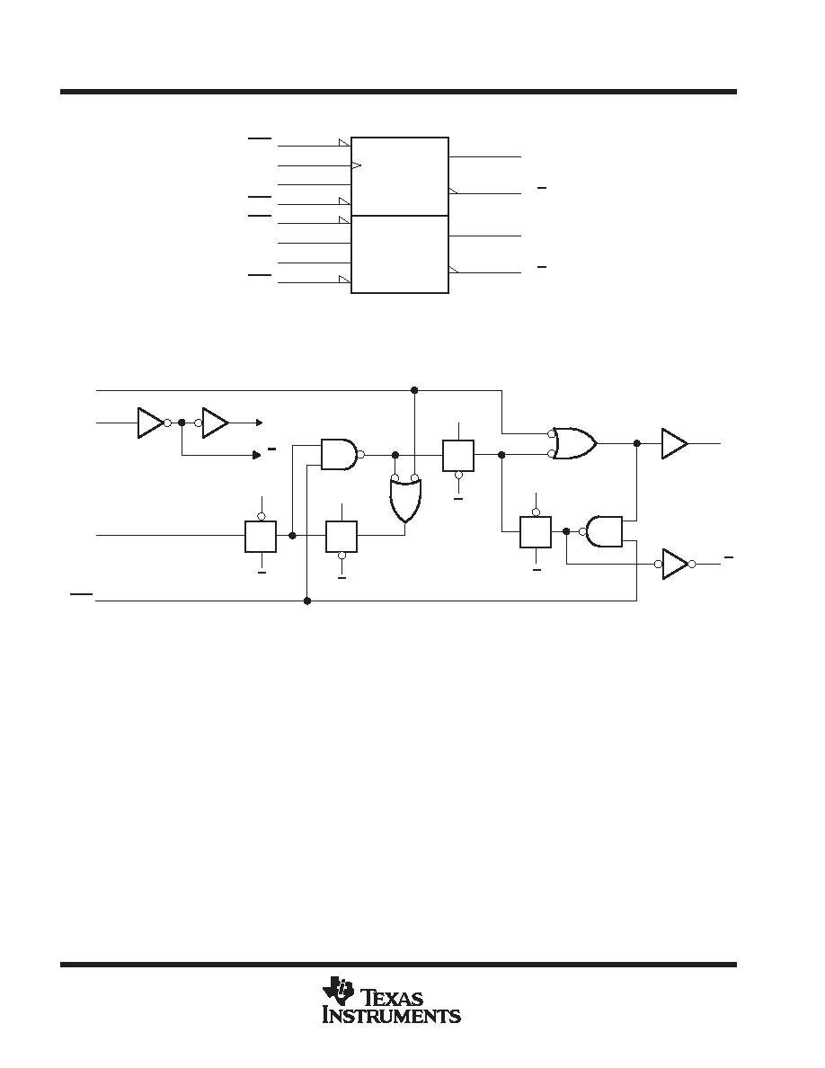
logic symbol
S
4
3
5
1D
2
R
1
9
10
11
12
13
6
8
1PRE
1CLK
1D
2PRE
1CLR
2CLK
2D
2CLR
1Q
2Q
C1
This symbol is in accordance with ANSI/IEEE Std 91-1984 and IEC Publication 617-12.
Pin numbers shown are for the D, J, N, PW, and W packages.
logic diagram (positive logic)
PRE
CLK
D
CLR
Q
C
TG
absolute maximum ratings over operating free-air temperature range
Supply voltage range, VCC
–0.5 V to 7 V
. . . . . . . . . . . . . . . . . . . . . . . . . . . . . . . . . . . . . . . . . . . . . . . . . . . . . . . . . .
Input clamp current, IIK (VI < 0 or VI > VCC) (see Note 1)
±20 mA
. . . . . . . . . . . . . . . . . . . . . . . . . . . . . . . . . . . .
Output clamp current, IOK (VO < 0 or VO > VCC) (see Note 1)
±20 mA
. . . . . . . . . . . . . . . . . . . . . . . . . . . . . . . .
Continuous output current, IO (VO = 0 to VCC)
±25 mA
. . . . . . . . . . . . . . . . . . . . . . . . . . . . . . . . . . . . . . . . . . . . . .
Continuous current through VCC or GND
±50 mA
. . . . . . . . . . . . . . . . . . . . . . . . . . . . . . . . . . . . . . . . . . . . . . . . . . .
Package thermal impedance,
θJA (see Note 2): D package
127
°C/W
. . . . . . . . . . . . . . . . . . . . . . . . . . . . . . . . . .
N package
78
°C/W
. . . . . . . . . . . . . . . . . . . . . . . . . . . . . . . . . . .
PW package
170
°C/W
. . . . . . . . . . . . . . . . . . . . . . . . . . . . . . . .
Storage temperature range, Tstg
–65
°C to 150°C
. . . . . . . . . . . . . . . . . . . . . . . . . . . . . . . . . . . . . . . . . . . . . . . . . . .
Stresses beyond those listed under “absolute maximum ratings” may cause permanent damage to the device. These are stress ratings only, and
functional operation of the device at these or any other conditions beyond those indicated under “recommended operating conditions” is not
implied. Exposure to absolute-maximum-rated conditions for extended periods may affect device reliability.
NOTES:
1. The input and output voltage ratings may be exceeded if the input and output current ratings are observed.
2. The package thermal impedance is calculated in accordance with JESD 51, except for through-hole packages, which use a trace
length of zero.
相关PDF资料 |
PDF描述 |
|---|---|
| SN54LS01W | LS SERIES, QUAD 2-INPUT NAND GATE, CDFP14 |
| SN54LS01FK | LS SERIES, QUAD 2-INPUT NAND GATE, CQCC20 |
| SN54LS06FKR | LS SERIES, HEX 1-INPUT INVERT GATE, CQCC20 |
| SN54LS112FK | LS SERIES, DUAL NEGATIVE EDGE TRIGGERED J-K FLIP-FLOP, COMPLEMENTARY OUTPUT, CQCC20 |
| SN54LS112J | LS SERIES, DUAL NEGATIVE EDGE TRIGGERED J-K FLIP-FLOP, COMPLEMENTARY OUTPUT, CDIP16 |
相关代理商/技术参数 |
参数描述 |
|---|---|
| SN54HCU04J | 制造商:Texas Instruments 功能描述:HEX INVERTER - Rail/Tube 制造商:Texas Instruments 功能描述:Inverter 6-Element CMOS 14-Pin CDIP Tube |
| SN54L00W | 制造商:MAJOR 功能描述: |
| SN54L46J | 制造商:Rochester Electronics LLC 功能描述:- Bulk |
| SN54L51J | 制造商:Texas Instruments 功能描述: |
| SN54L74T | 制造商:Texas Instruments 功能描述:Flip Flop, Dual, D Type, 14 Pin, Metal, Flat Pack |
发布紧急采购,3分钟左右您将得到回复。