- 您现在的位置:买卖IC网 > PDF目录373451 > SN54LS16 (Texas Instruments, Inc.) Hex Inverter Buffers/Drivers With Open-Collector High Voltage Outputs(六反相缓冲器/驱动器(集电极高电压开路输出)) PDF资料下载
参数资料
| 型号: | SN54LS16 |
| 厂商: | Texas Instruments, Inc. |
| 英文描述: | Hex Inverter Buffers/Drivers With Open-Collector High Voltage Outputs(六反相缓冲器/驱动器(集电极高电压开路输出)) |
| 中文描述: | 六角逆变器缓冲器/配合开放的驱动,集电极输出高电压(六反相缓冲器/驱动器(集电极高电压开路输出)) |
| 文件页数: | 3/14页 |
| 文件大小: | 434K |
| 代理商: | SN54LS16 |
SDLS020E MAY 1990 REVISED FEBRUARY 2004
3
POST OFFICE BOX 655303
DALLAS, TEXAS 75265
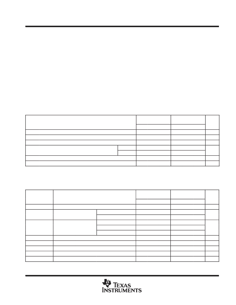
absolute maximum ratings over operating free-air temperature range (unless otherwise noted)
Supply voltage, V
CC
Input voltage, V
I
(see Note 1)
Output voltage, V
O
(see Notes 1 and 2): SN54LS06, SN74LS06
7 V
7 V
30 V
15 V
. . . . . . . . . . . . . . . . . . . . . . . . . . . . . . . . . . . . . . . . . . . . . . . . . . . . . . . . . . . . . . . . . . . . . . . .
. . . . . . . . . . . . . . . . . . . . . . . . . . . . . . . . . . . . . . . . . . . . . . . . . . . . . . . . . . . . . . . . .
. . . . . . . . . . . . . . . . . . . . . . . . . . . . . . . . .
. . . . . . . . . . . . . . . . . . . . . . . . . . . . . . . . . . . . . . . . . . . .
. . . . . . . . . . . . . . . . . . . . . . . . . . . . . . . . . . .
DB package
. . . . . . . . . . . . . . . . . . . . . . . . . . . . . . . . .
N package
. . . . . . . . . . . . . . . . . . . . . . . . . . . . . . . . . . .
NS package
. . . . . . . . . . . . . . . . . . . . . . . . . . . . . . . . .
. . . . . . . . . . . . . . . . . . . . . . . . . . . . . . . . . . . . . . . . . . . . . . . . . . .
SN74LS16
Package thermal impedance,
θ
JA
(see Note 3): D package
86
°
C/W
96
°
C/W
80
°
C/W
76
°
C/W
Storage temperature range, T
stg
Stresses beyond those listed under “absolute maximum ratings” may cause permanent damage to the device. These are stress ratings only, and
functional operation of the device at these or any other conditions beyond those indicated under “recommended operating conditions” is not
implied. Exposure to absolute-maximum-rated conditions for extended periods may affect device reliability.
NOTES:
1. All voltage values are with respect to GND.
2. This is the maximum voltage that should be applied to any output when it is in the off state.
3. The package thermal impedance is calculated in accordance with JESD 51-7.
65
°
C to 150
°
C
recommended operating conditions (see Note 4)
SN54LS06
SN74LS06
SN74LS16
UNIT
MIN
NOM
MAX
MIN
NOM
MAX
VCC
VIH
VIL
Supply voltage
4.5
5
5.5
4.75
5
5.25
V
High-level input voltage
2
2
V
Low-level input voltage
0.8
0.8
V
VOH
High-level output voltage
’LS06
30
30
V
SN74LS16
15
IOL
TA
NOTE 4: All unused inputs of the device must be held at VCC or GND to ensure proper device operation. Refer to the TI application report,
Implications of Slow or Floating CMOS Inputs
, literature number SCBA004.
Low-level output current
30
40
mA
°
C
Operating free-air temperature
55
125
0
70
electrical characteristics over recommended operating free-air temperature range (unless
otherwise noted)
PARAMETER
TEST CONDITIONS
SN54LS06
SN74LS06
SN74LS16
TYP§
UNIT
MIN
TYP§
MAX
MIN
MAX
VIK
VCC = MIN,
II = 12 mA
1.5
1.5
V
IOH
VCC = MIN,
VIL = 0.8 V
’LS06,
VOH = 30 V
VOH = 15 V
0.25
0.25
mA
SN74LS16,
0.25
IOL = 16 mA
IOL = 30 mA
IOL = 40 mA
0.25
0.4
0.25
0.4
VOL
VCC = MIN,
VIH = 2 V
0.7
V
0.7
II
IIH
IIL
ICCH
ICCL
VCC = MAX,
VCC = MAX,
VCC = MAX,
VCC = MAX
VCC = MAX
VI = 7 V
VI = 2.4 V
VI = 0.4 V
1
1
mA
μ
A
mA
20
20
0.2
0.2
18
18
mA
60
60
mA
For conditions shown as MIN or MAX, use the appropriate value specified under
recommended operating conditions
.
§All typical values are at VCC = 5 V, and TA = 25
°
C.
The SN74LS16 is obsolete
and is no longer supplied.
相关PDF资料 |
PDF描述 |
|---|---|
| SN54LS171 | QUADRUPLE D-TYPE FLIP-FLOPS WITH CLEAR |
| SN54LS171FK | QUADRUPLE D-TYPE FLIP-FLOPS WITH CLEAR |
| SN54LS171J | QUADRUPLE D-TYPE FLIP-FLOPS WITH CLEAR |
| SN54LS171W | QUADRUPLE D-TYPE FLIP-FLOPS WITH CLEAR |
| SN54LS183 | Dual Carry-Save Full Adders(双进位保留全加器) |
相关代理商/技术参数 |
参数描述 |
|---|---|
| SN54LS160A/BEA | 制造商:Rochester Electronics LLC 功能描述: |
| SN54LS160AJ | 制造商:Texas Instruments 功能描述: |
| SN54LS161AJ | 制造商:Texas Instruments 功能描述:Counter Single 4-Bit Sync Binary UP 16-Pin CDIP Tube 制造商:Texas Instruments 功能描述:COUNTER SGL 4BIT SYNC BINARY UP 16CDIP - Rail/Tube 制造商:Texas Instruments 功能描述:4 BIT SYNC BINARY COUNTER |
| SN54LS162W | 制造商:Texas Instruments 功能描述: |
| SN54LS163AJ | 制造商:Texas Instruments 功能描述:Counter Single 4-Bit Sync Binary UP 16-Pin CDIP Tube 制造商:Rochester Electronics LLC 功能描述:- Bulk 制造商:Texas Instruments 功能描述:SYNC 4-BIT BINARY COUNTER - Rail/Tube 制造商:Motorola Inc 功能描述:Counter, Up, 4 Bit Binary, 16 Pin, Ceramic, DIP |
发布紧急采购,3分钟左右您将得到回复。